QUANTAX EDS for TEM
XFlash® 7T - Seeing Nano in Color: STEM EDS in TEM and SEM
QUANTAX EDS for TEM

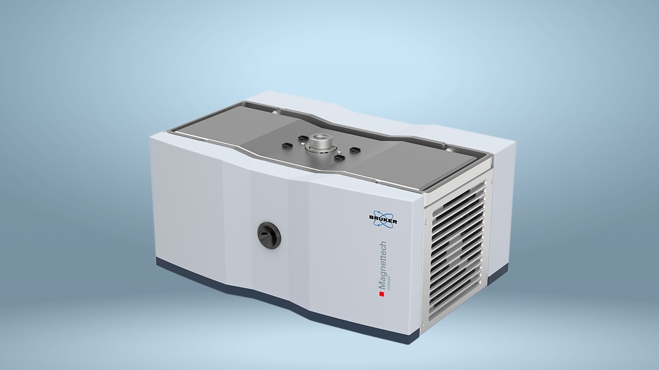
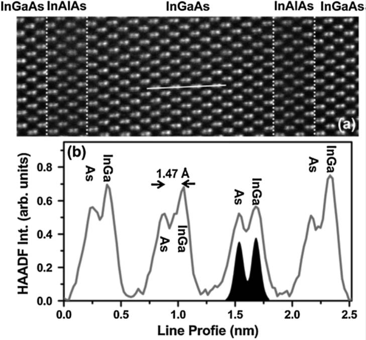
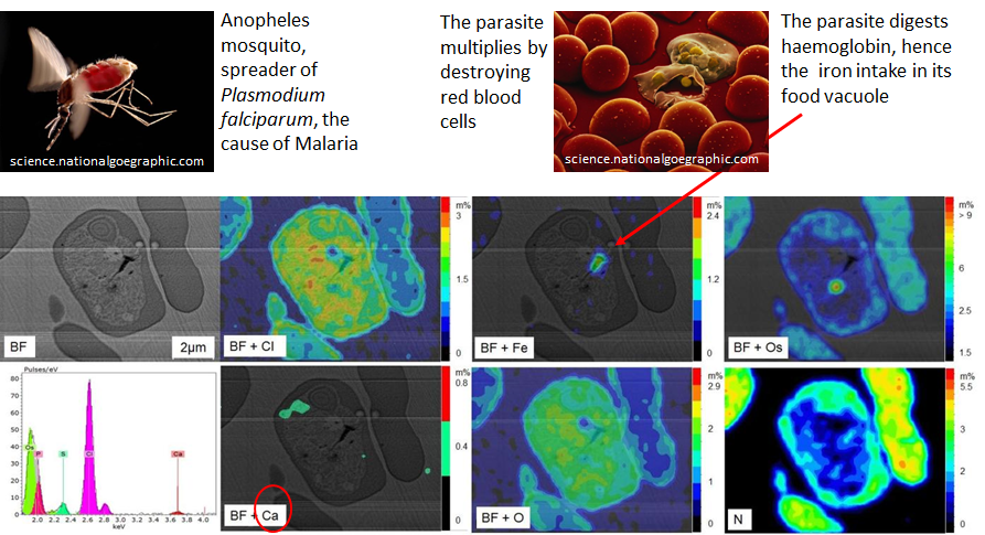
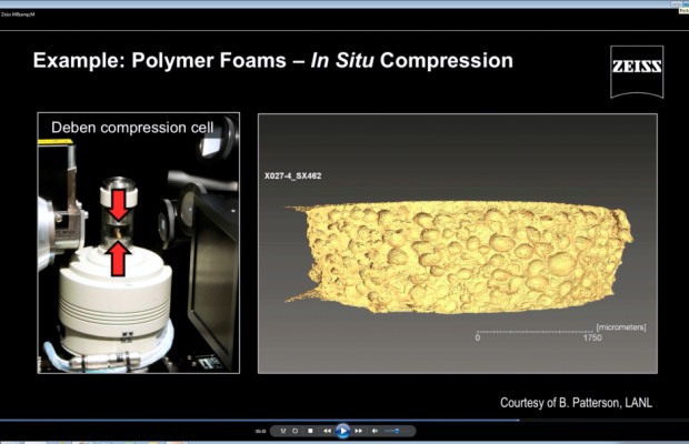
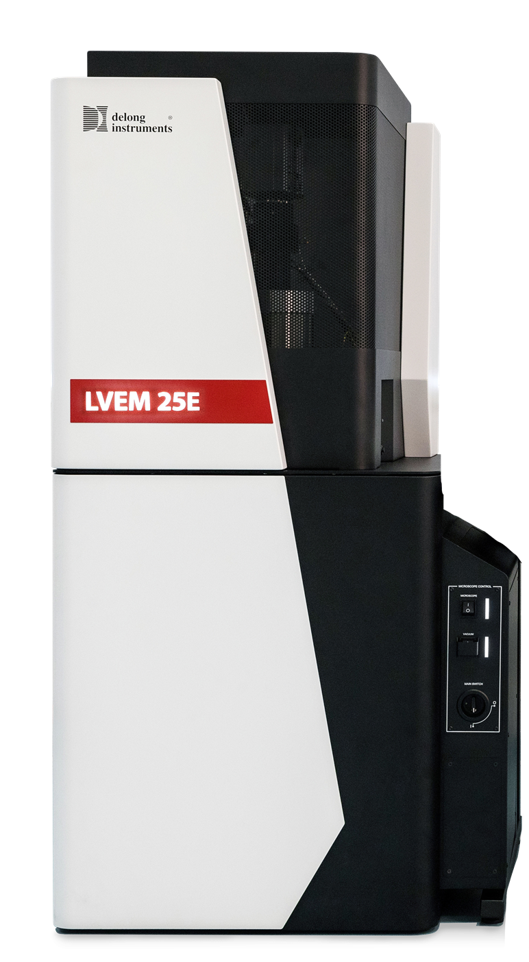
Single Atoms and Nanostructures

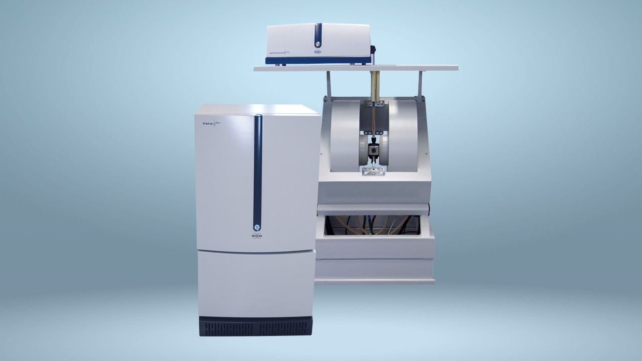
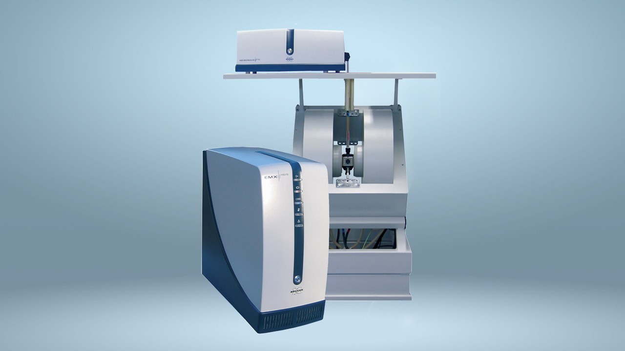
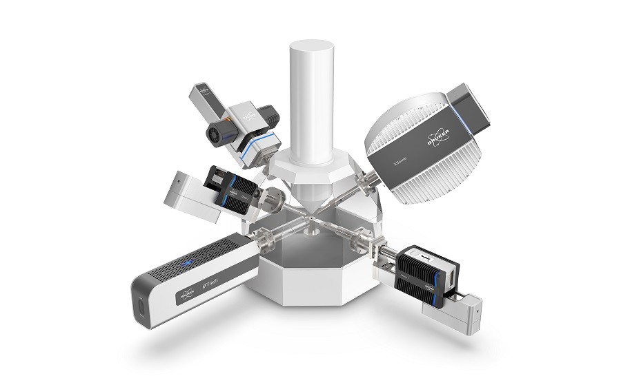
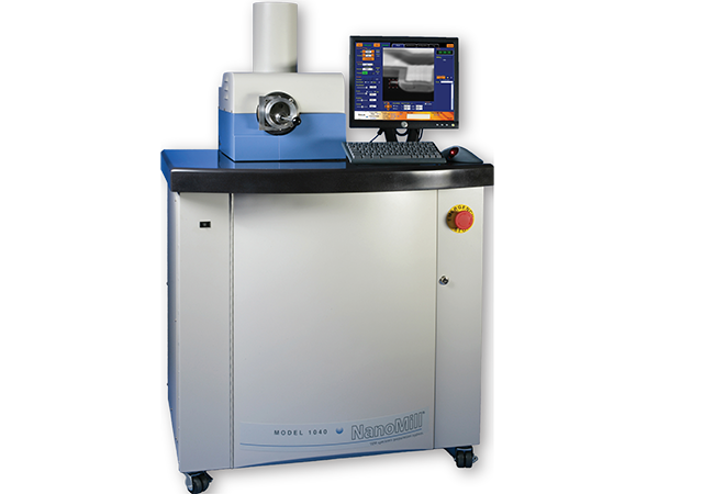
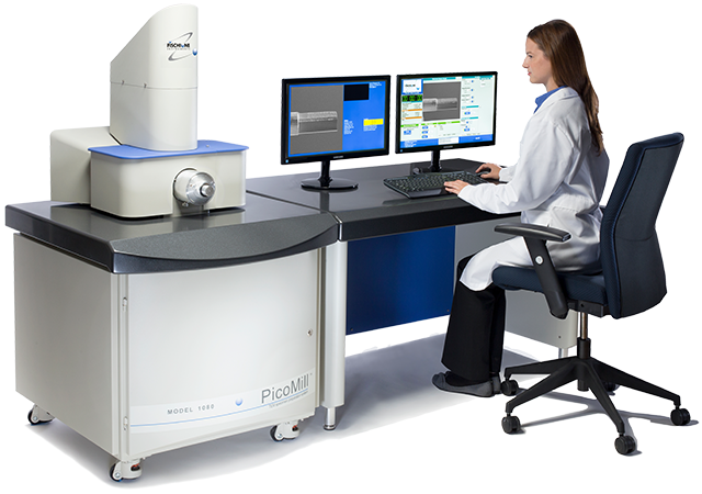
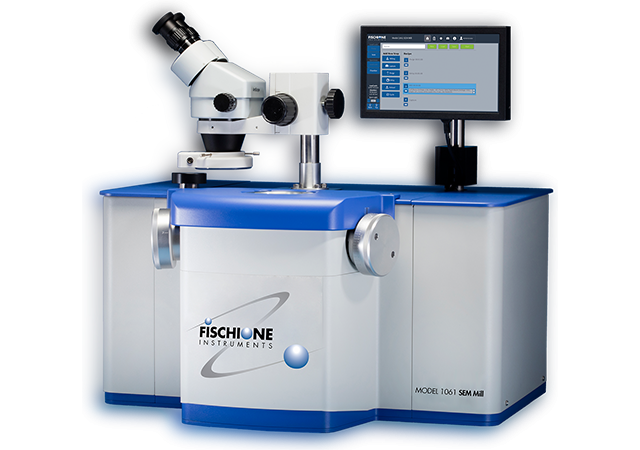
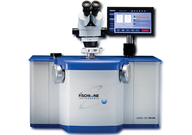
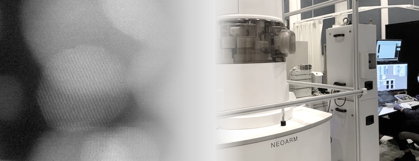
Get the Best Possible Results for each Specific Microscope

80keV

Unprecedented upper energy limit
Unequivocally identify and quantify all present elements

Å

Stable resolution
Map periodic structures (atom, layers) with high stability and using enhanced drift correction features

3 TEM-quantification models

Succeed in TEM, STEM and T-SEM with easy-to-use powerful quantification based on theoretical and experimental Cliff-Lorimer factors, as well as Zeta-factor interpolation

Element Analysis in Transmission Electron Microscopy on the Nanometer Scale

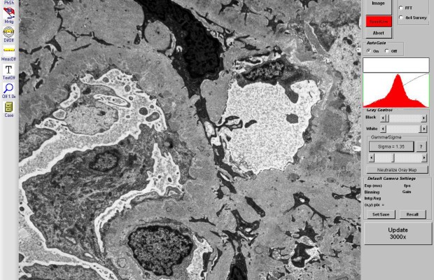
Flexible and easy-to-use analysis software package ESPRIT with an open user interface: you see what you do.

Off-line analysis option with individual or LAN access for student or laboratory networks.

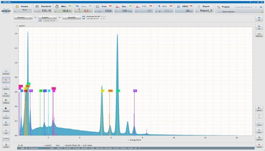
Sophisticated most seasoned quantitative energy dispersive X-ray spectroscopy (EDS) for complete data mining includes: 

  • Options for quantification steps: default suggestions for easy use, indvidual setup, detailed modification and saving/reloading of recipes
  • 3 different quantification approaches are covering all possible scenarios based on theoretical and experimental Cliff-Lorimer factors as well as Zeta-factors and the interpolation of missing Zeta-factors
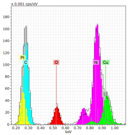
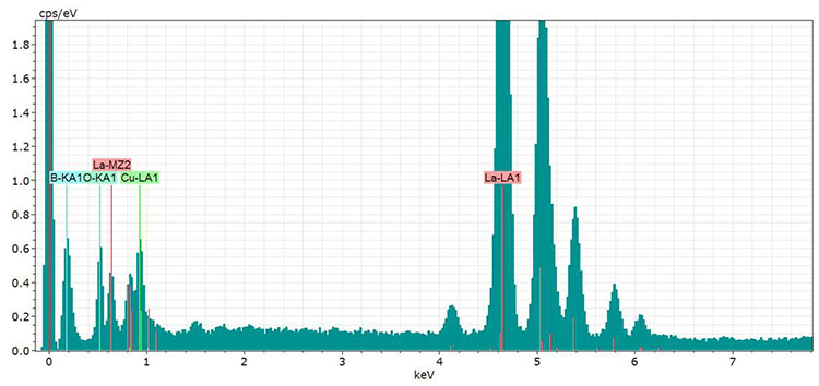
  • TEM-specific high energy element lines above 40 keV available for quantification ensuring unambiguous results
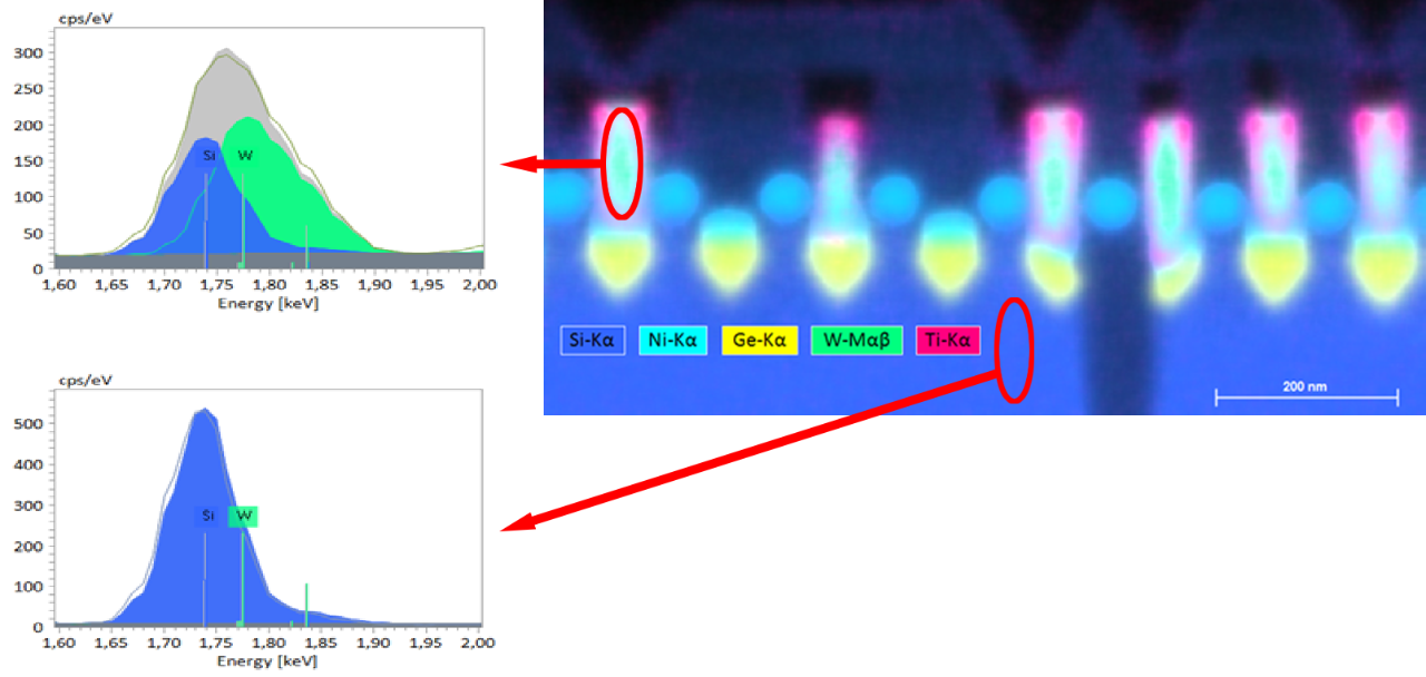
  • Choice of 3 vital background models: a physical one for bulk and a physical one for thin lamellae as well as a mathematical model
  • Absorption correction included in the Cliff-Lorimer quantification already

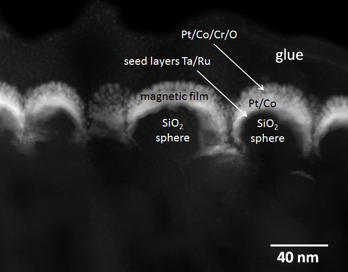
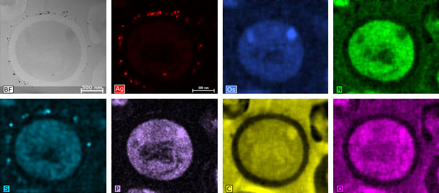
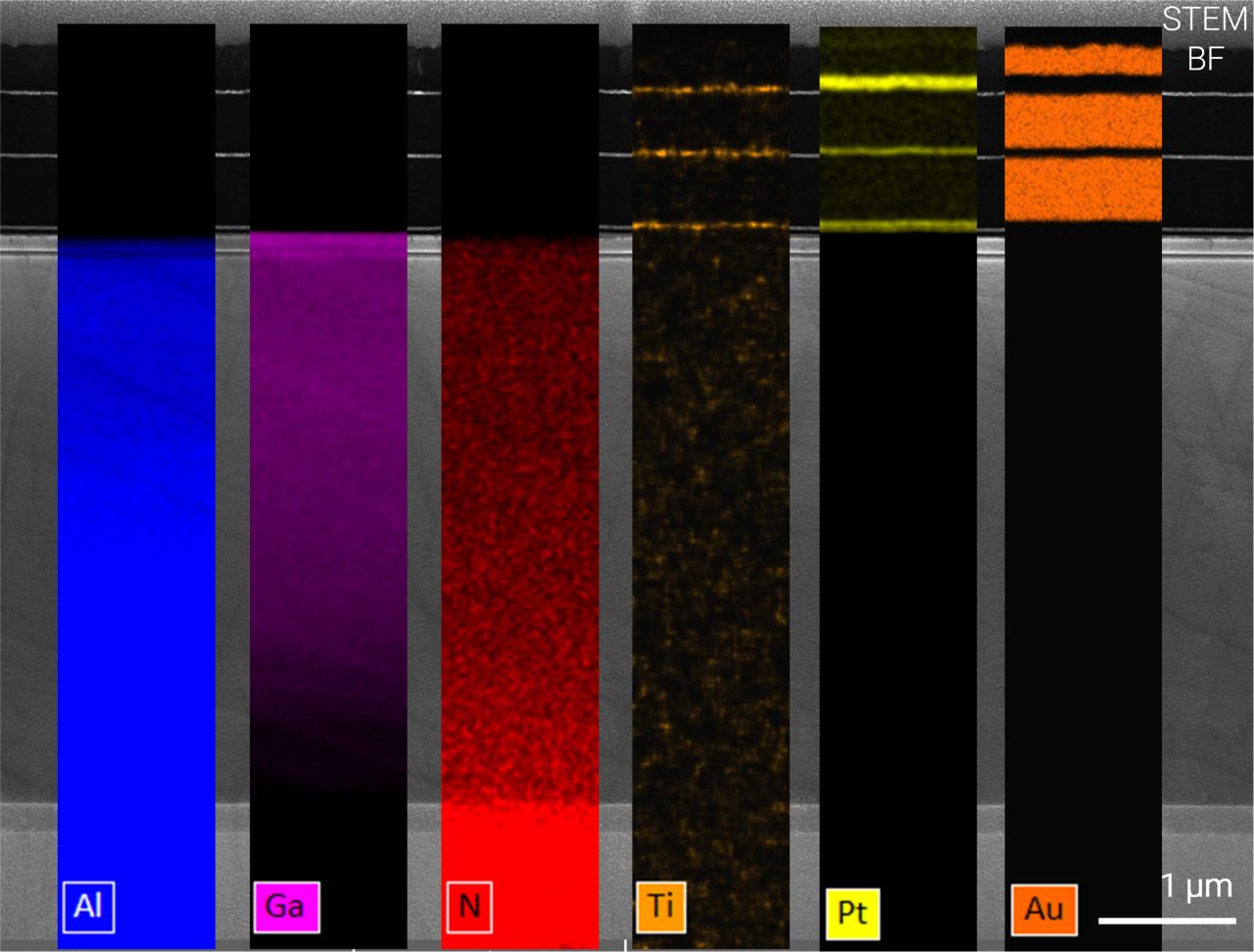
High-resolution Element Distribution Analysis of Electron Transparent Samples in TEM, STEM and SEM (T-SEM)

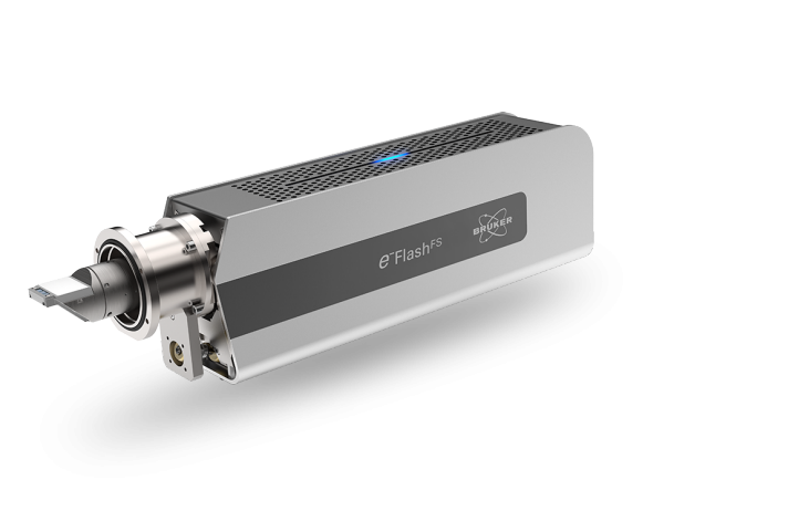
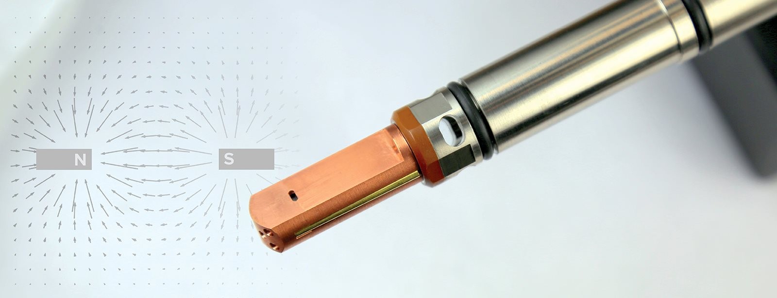
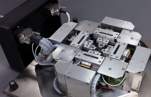
  • Long standing expertise in EDS ensures the configuration of the best solution for your specific microscope (STEM, TEM or SEM) thanks to slim-line detector design and geometrical optimization for each microscope pole piece and EDS flange type
  • Maximum collection and take-off angle allow fast and highly sensitive data acquisition
  • Fast-moving stable detector stage
  • A special drift correction routine for periodic features ensures successful EDS on the nanoscale
  • Time resolved data acquisition for in-situ experiments suitable for saving a stream of changing data, f.e. at elevated temperatures
  • Automation of data acquisition and analysis processes using the scripting and API options for generation of specific analysis jobs and batch processing
  • Clean data needing no or minimal post-acquisition corrections due to avoiding mechanical and electromagnetic interference completely and avoiding or keeping to a minimum specimen tilt, absorption, shadowing and system peaks
  • Most seasoned quantification for EDS data from electron transparent specimens on the market provides thorough data mining with unambiguous results
  • Highest quality assistance and training due to long standing experience in TEM for using your system to its full power


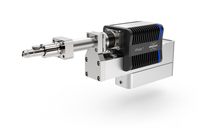
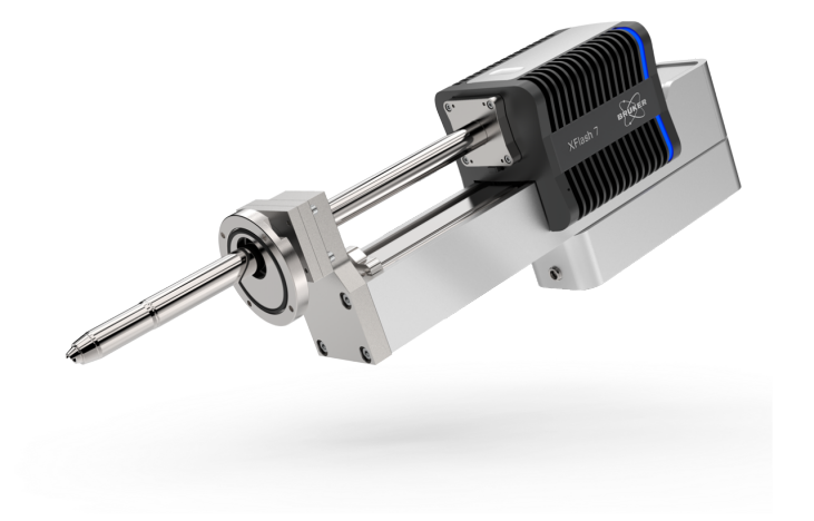
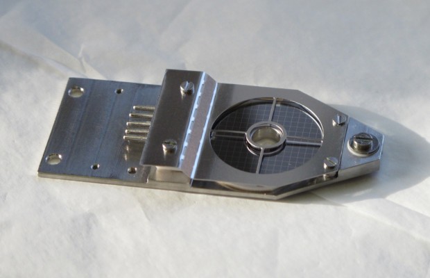
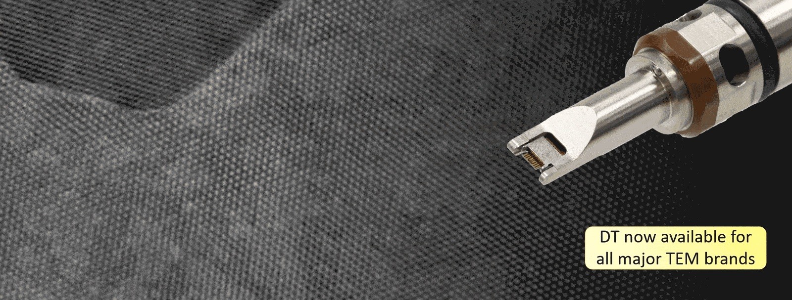
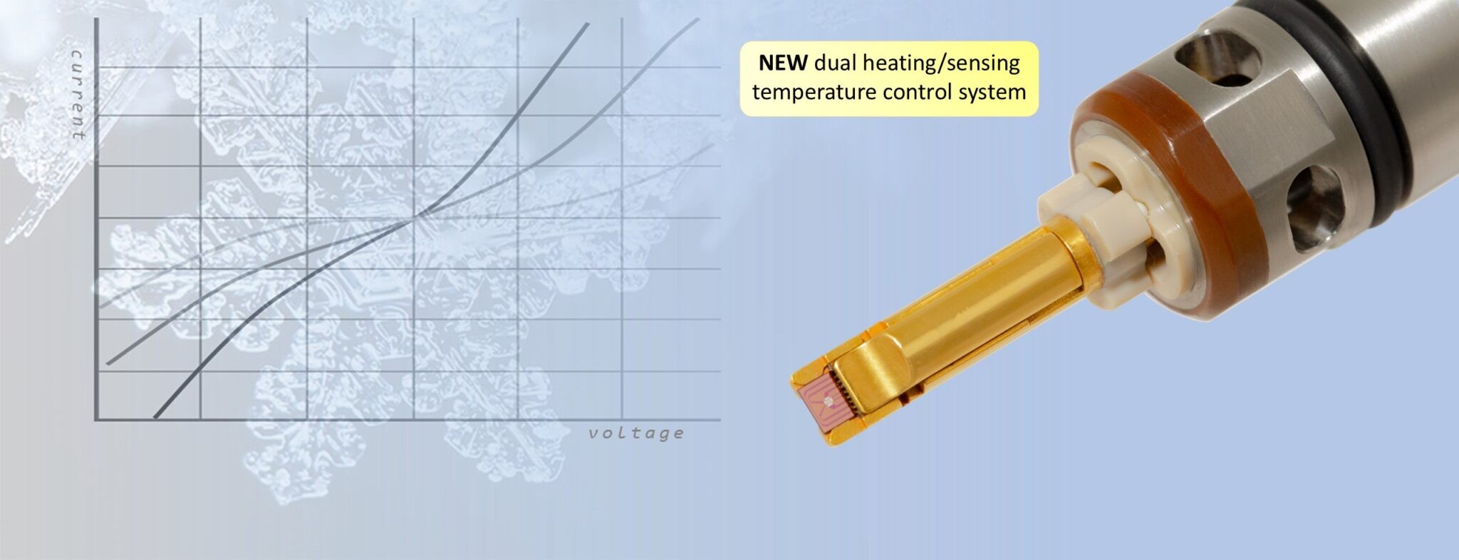
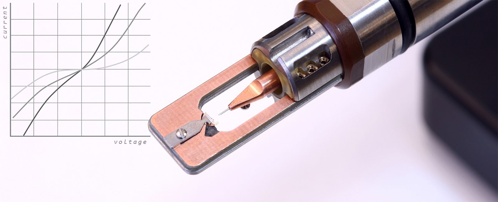
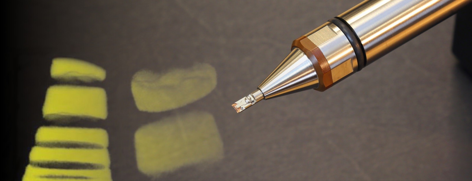
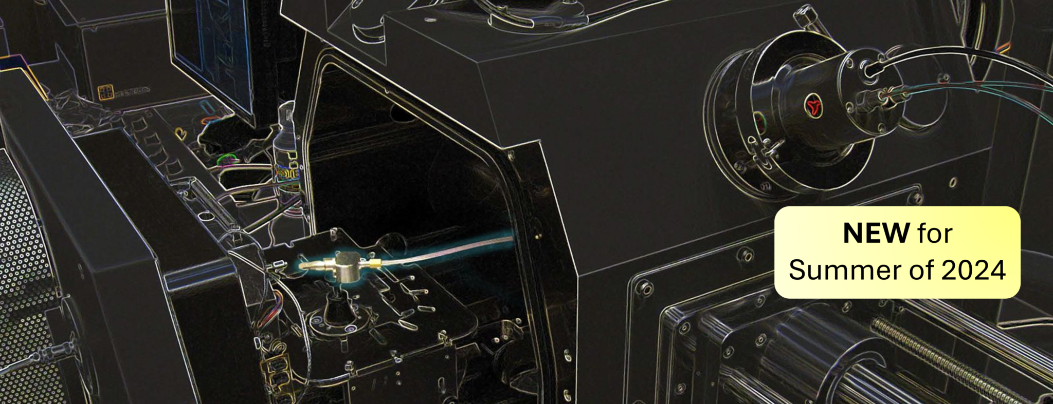
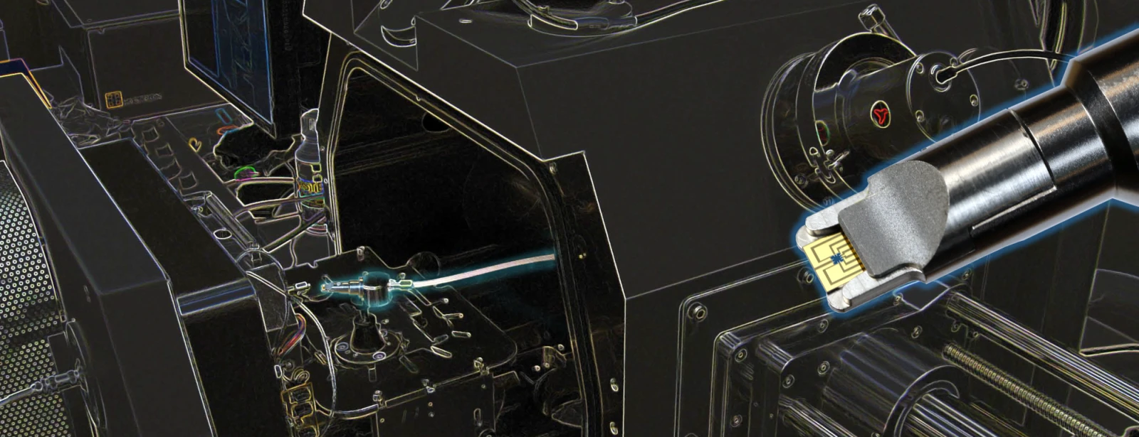
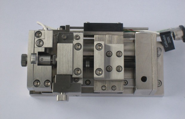
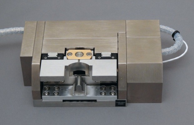
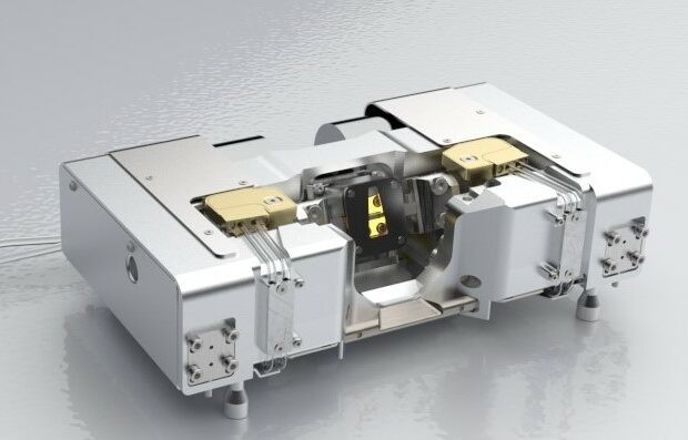
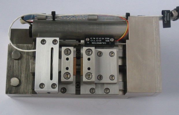
Ultimative Results with the Latest XFlash® 7 EDS Detectors for TEM

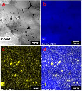
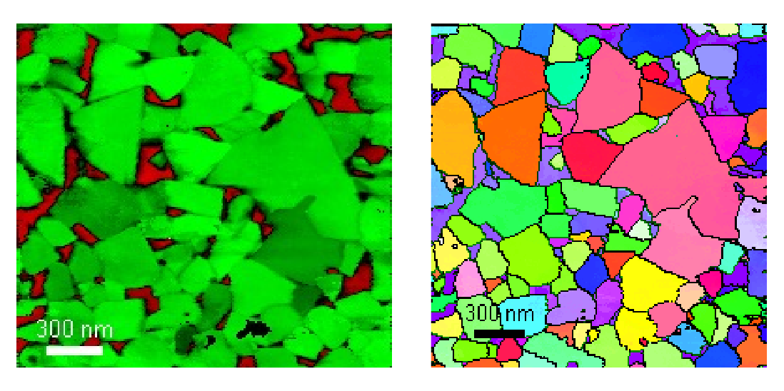
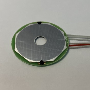
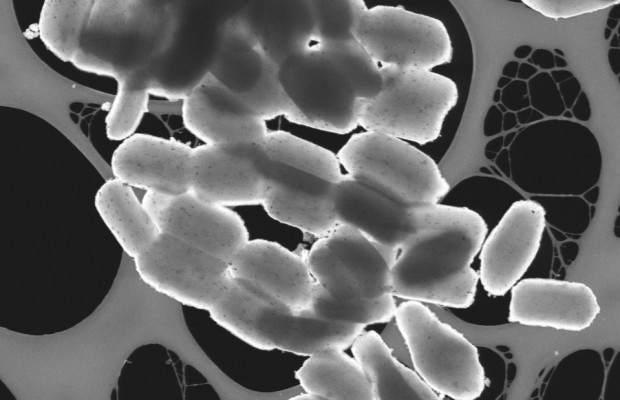
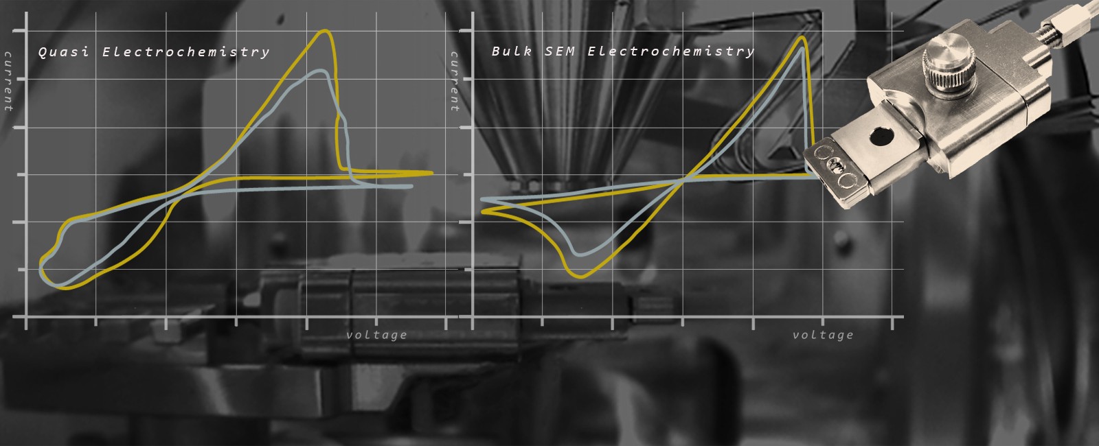
EDS Analyses of Coated Li-ion Battery Cathode Particle

The capacitance retention of NCM cathode material of batteries (SSB and LIB) can be improved by coating structures. To control the performance of these nanometer-thick coatings, their elemental distribution must be known. We present a SEM-based solution of EDS analysis achieving nanometer resolution on micrometer-sized cathode particles with irregular surfaces and compare it to TEM EDS.

Battery Analysis with TEM EDS

EDS analysis of battery
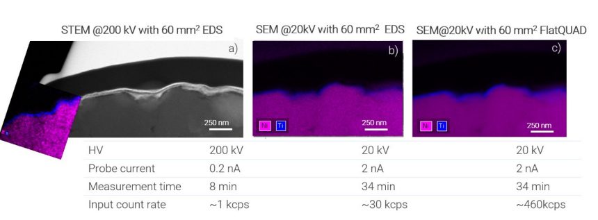
© Image and sample courtesy of Michael Malaki, Shamail Ahmed; Material Science center, Faculty of physics, Philipps University Marburg

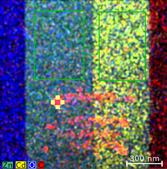
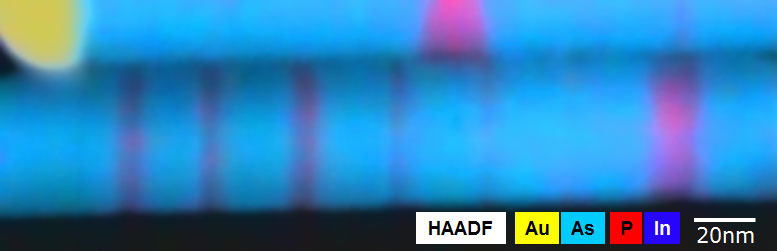
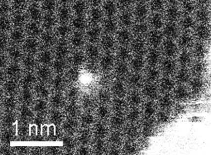
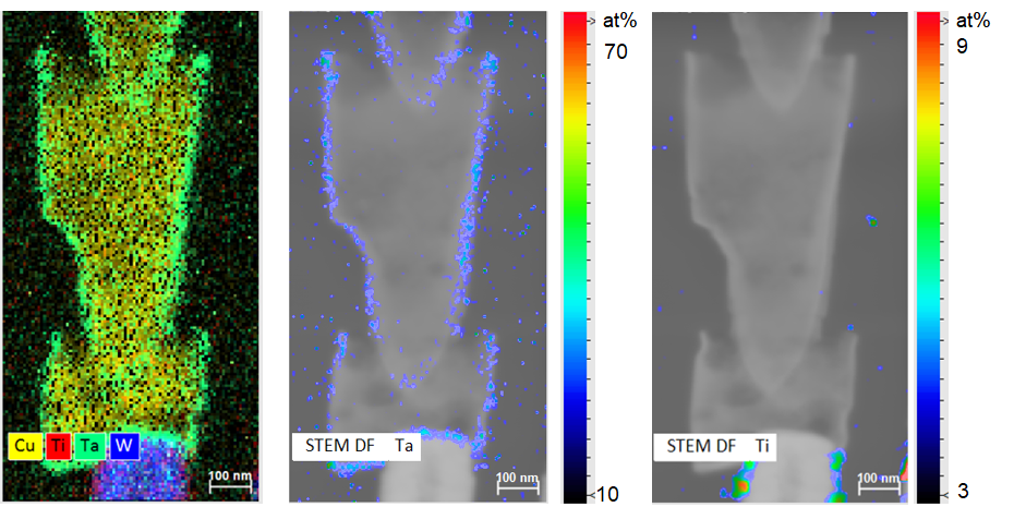
Fields of Application of Elemental Analysis on TEM

Semiconductors
 
Deconvolution results at low X-ray energy of a spectrum obtained from a NiSi(Pt)

Quantification of the Pt Concentration in a NiSi(Pt)-NiSi2 Semiconductor Structure

This application example shows EDS data from the epitaxial growth of a Pt alloyed NiSi thin film and the quantification of a few at% of Pt alloyed in NiSi. NiSi is used for nm-sized metallization structures in semiconductor devices like MOSFETs.
Combined element maps of a layered system

Chemical Phase Analysis of a Layered Structure

It can be advantageous to check hyperspectral images for the existence of chemical phases without applying prior knowledge. Bruker’s ESPRIT AutoPhase automatically finds specimen regions of similar composition by analyzing a HyperMap based on Principle Component Analysis of the spectra. 
Mixed element map of nanowires

Chemical Characterization of Nanowires

Nanostructures, such as nanowires and nanorods and functionalized nanovehicles are of growing interest for various applications in nanotechnology, be that nano-electronics or drug delivery in the human body.


Single silicon atom in graphene

Identifiying a Single Atom on Graphene

Not only is it the highest art of EDS to obtain spectra of a single atom, but it can also provide valuable new information on the excitation properties of specific elements.
High angle annular darkfield image of an interconnect structure

Chemical Composition of Semiconductor Interconnects

Standard energy dispersive X-ray spectroscopy (EDS or EDX) using detector areas of 30mm2 on conventional scanning transmission electron microscopes (STEM) can deliver element mappings with nm resolution within a few minutes. The condition is, that the detector head is small enough (in slim-line design) to get as close to the specimen for (high solid angle) and as high above the specimen (for high take-off angle) as possible. The latter helps to avoid shadowing and absorption effects.
RAM microchip elemental distribution map

High Resolution Mapping of a Semiconductor RAM Microchip Using STEM-EDS in SEM (T-SEM)

Element distribution mapping of semiconductor nanostructures with X-ray based methods is not always straight forward. The need of nanoscale spatial resolution and X-ray peak overlaps are common challenges when investigating semiconductor materials. Sometimes it can be beneficial to use the SEM instead of expensive TEM tools and time for characterization.


Nanomaterials
 
Bright field image and single element maps of a yeast cell

Mapping a Magnetic Nanostructure

The specimen consists of a SiO2 sphere coated with nm-thin layers of tantalum (Ta), ruthenium (Ru) and topmost a mixture of cobalt (Co), platinum (Pt), chromium (Cr) and oxygen (O).
HAADF image of Pd-Pt core shell particles

Qualitative and Quantitative Mapping of a Pd-Pt Core Shell Particle

Core shell particles play an increasingly important role in nanotechnology, particularily in catalysis. This application example presents element maps of a Pd-Pt core shell nano-particle.
HAADF image and intensity line scan of a InGaAS semiconductor structure

Atom Column EDS Analysis

Properties of a semiconductor are determined by its structure on the atomic level, e.g. by point defects. Using EDS mapping at highest possible resolution it is possible to locate and characterize such defects.


Bio/Soft Materials
 
 Spectrum of the LaB6 standard used for  Cliff-Lorimer factor calibration

Quantitative Analysis Using LaB6 as an Example

Lanthanum hexaboride (LaB6) is a very illustrative example for quantitative EDS analysis in S/TEM, since it contains two extremes, a very light element (B) and a heavy element (La).
Bright field image and single element maps of a yeast cell

EDS for Life Science

EDS in S/TEM is particularly useful if many elements in a material have to be determined at once. This is the case for quite a few life science applications.
Malaria parasite in human blood cell

Chemistry of a Malaria Parasite in Human Blood and Immunolabels in a Yeast Cell

Energy dispersive X-ray spectroscopy (EDX or EDS or EDXS) in transmission electron microscopy (STEM) can contribute valuable data in life science, for example for cell and tissue imaging. Silicon drift detectors, used for EDS, have become so sensitive in the lower energy region, that the detection of small amounts of light elements relevant for life science, such as calcium, oxygen, nitrogen and sulfur, is routinely possible now.


Webinars on EDS Elemental Mapping in TEM, STEM and SEM (T-SEM) 

XFlash 7 EDS detector series element analysis EDS
ON-DEMAND SESSION - 35 MINUTES

Introducing the XFlash® 7 EDS Detector

In this webinar we present the benefits of this new detector series and discuss specifics of microscope detector geometries. We also show examples of data acquisition and analysis across different fields of application. 
Element distribution in FIB lamella by SEM EDS
ON-DEMAND SESSION - 57 MINUTES

Optimizing Semiconductor-based LED Devices Using EDS of Electron Transparent Specimens in STEM/SEM

The understanding of semiconductor structures on the nanoscale mostly needs high-end analytical scanning transmission electron microscopy including the respective method combination and complex specimen preparation. Here UV-LEDs have been recently tested for skin-tolerant inactivation of SARS-CoV-2 and multi-resistant bacteria.
Significance of STEM-EDXS Analysis in the Characterization of Rechargeable Battery Components
ON-DEMAND SESSION - 49 MINUTES

Significance of STEM-EDXS Analysis in the Characterization of Rechargeable Battery Components

Discussing the use of STEM-EDXS to identify sulfur impurities inside nanopores and at grain boundaries that otherwise go undetected in EELS.


Resources & Publications


Learn more about EDS

Interested in learning more about EDS? Visit our explainer page: 


Diğer Ürünler
iMag sağlanan hizmetlerin iyileştirilmesi ve web sitesinde en iyi deneyimi yaşamanızı sağlamak için çerezleri kullanır.
close