Outstanding Spectral Resolution
Enhanced Analytical Accuracy and Precision
~ 4 eV
FWHM for Si-Kα
> 900 cps/nA
Count rate for C-Kα with an 80 Å multilayer
< 100 ppm
Detection limit for numerous elements
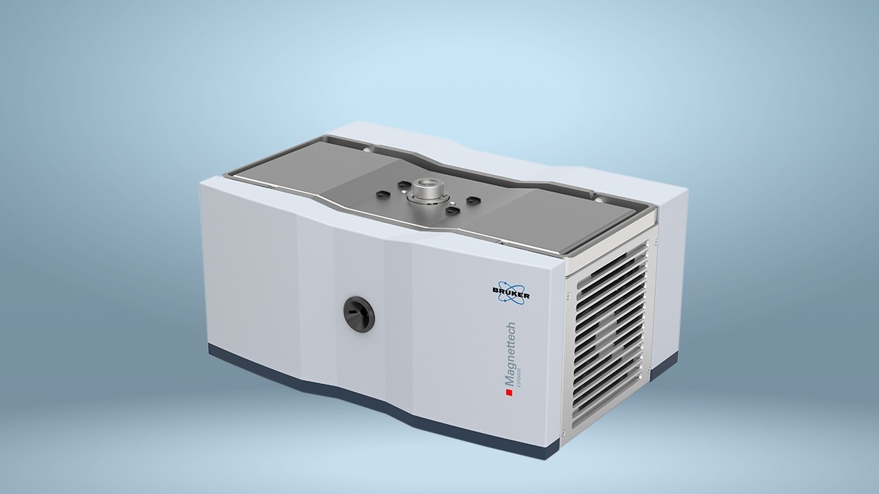
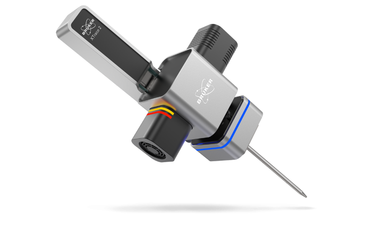
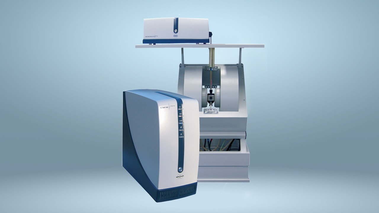
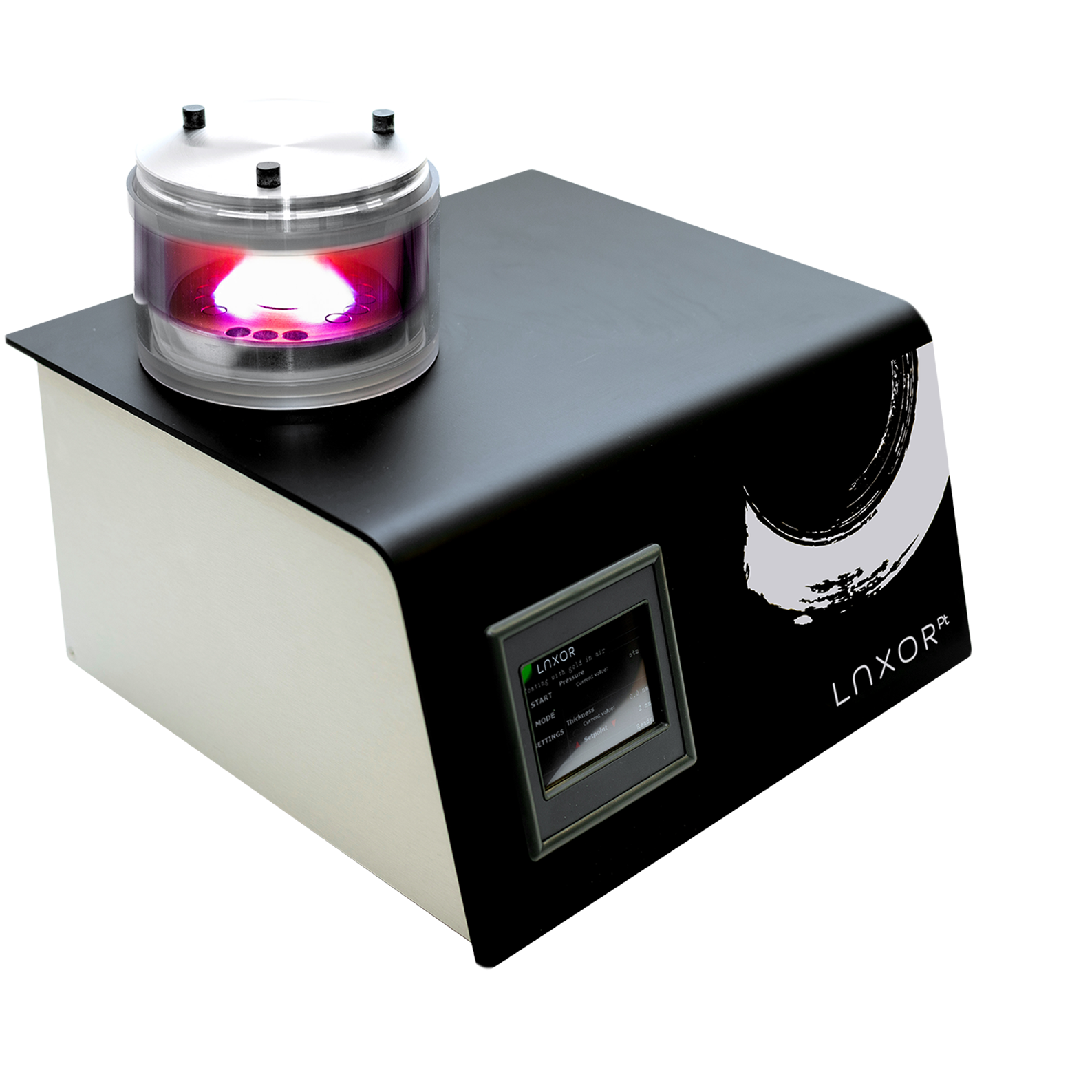
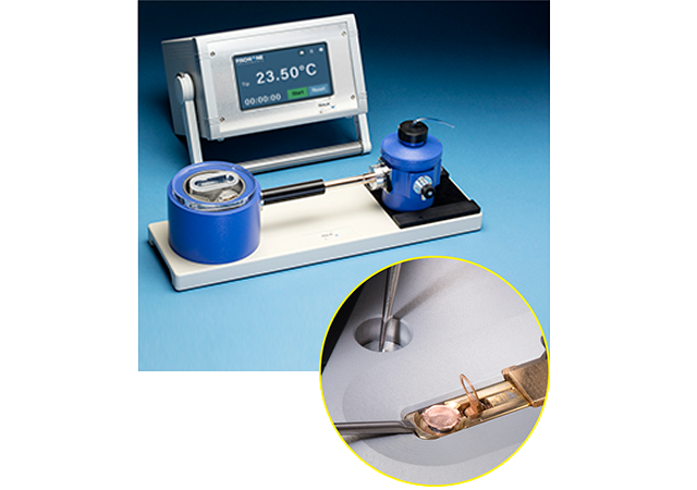
Complement Your SEM with the Benefits of an Electron Probe Micro Analyzer
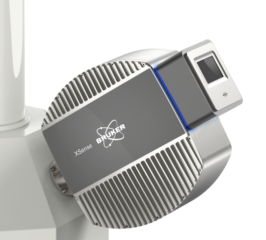
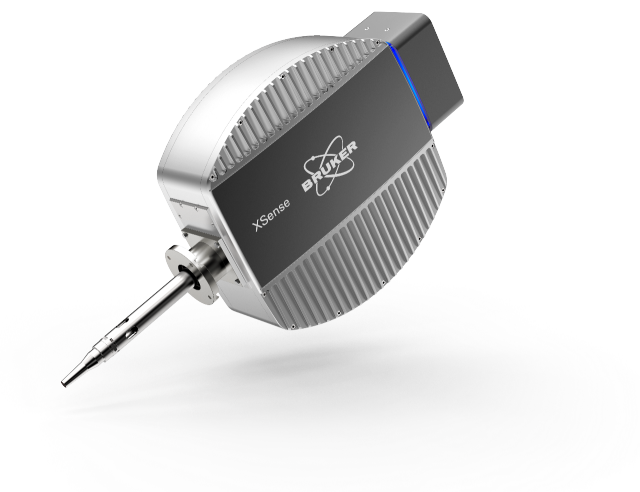
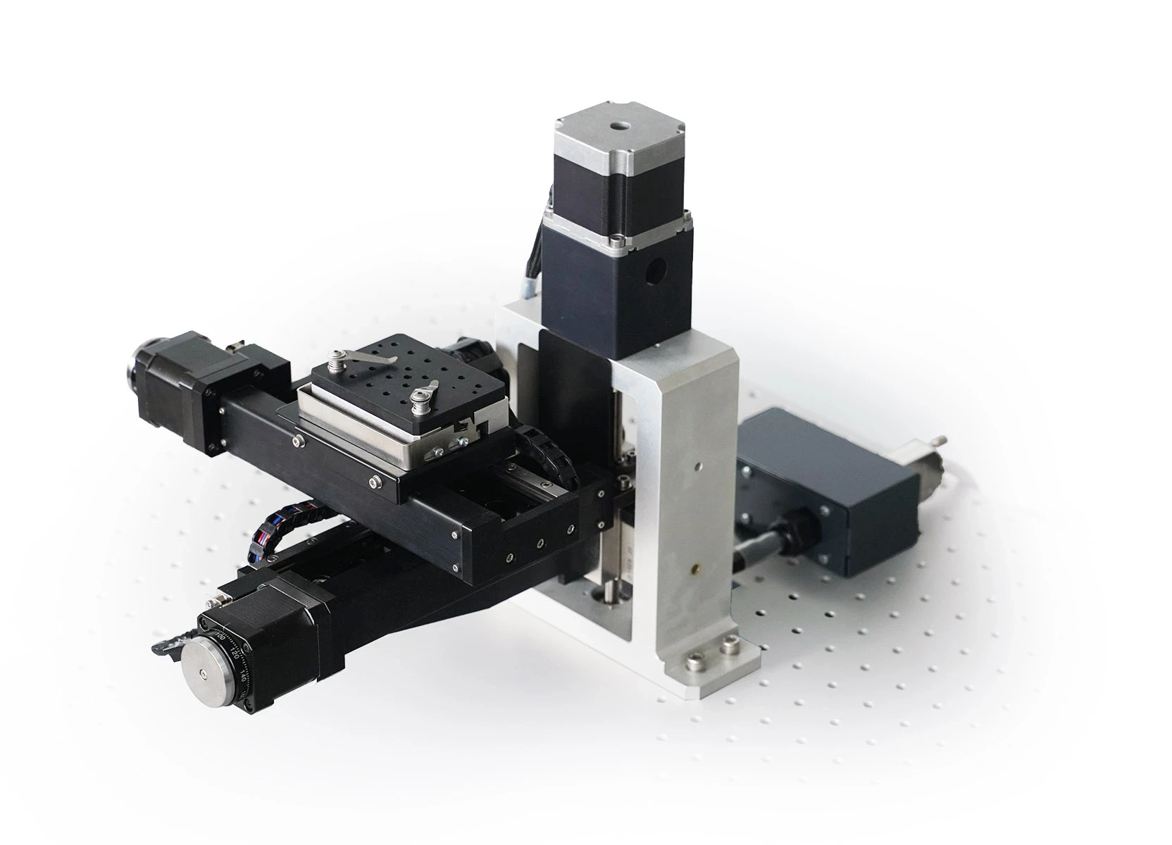
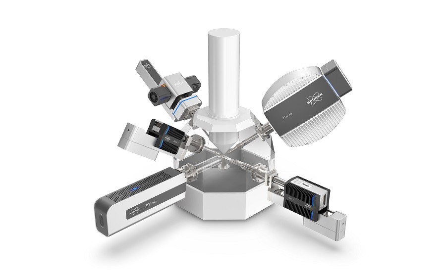
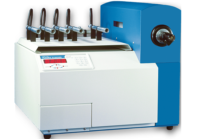
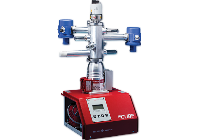
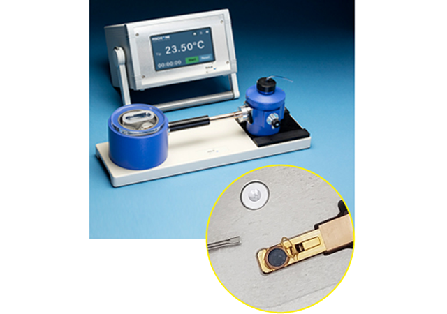
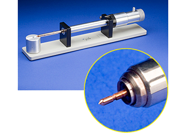
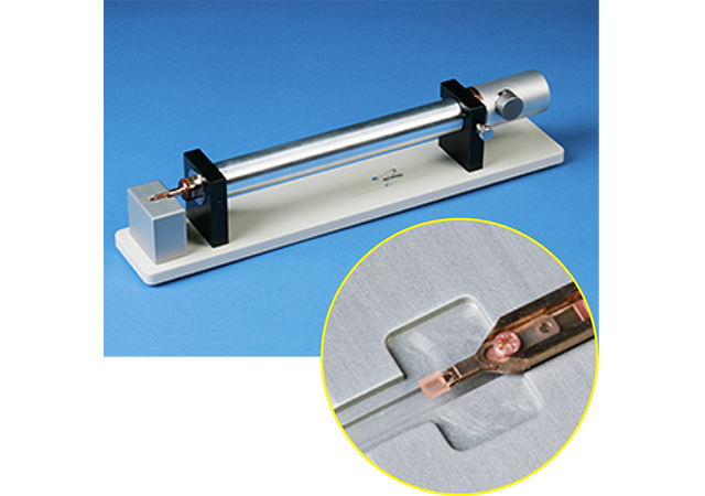
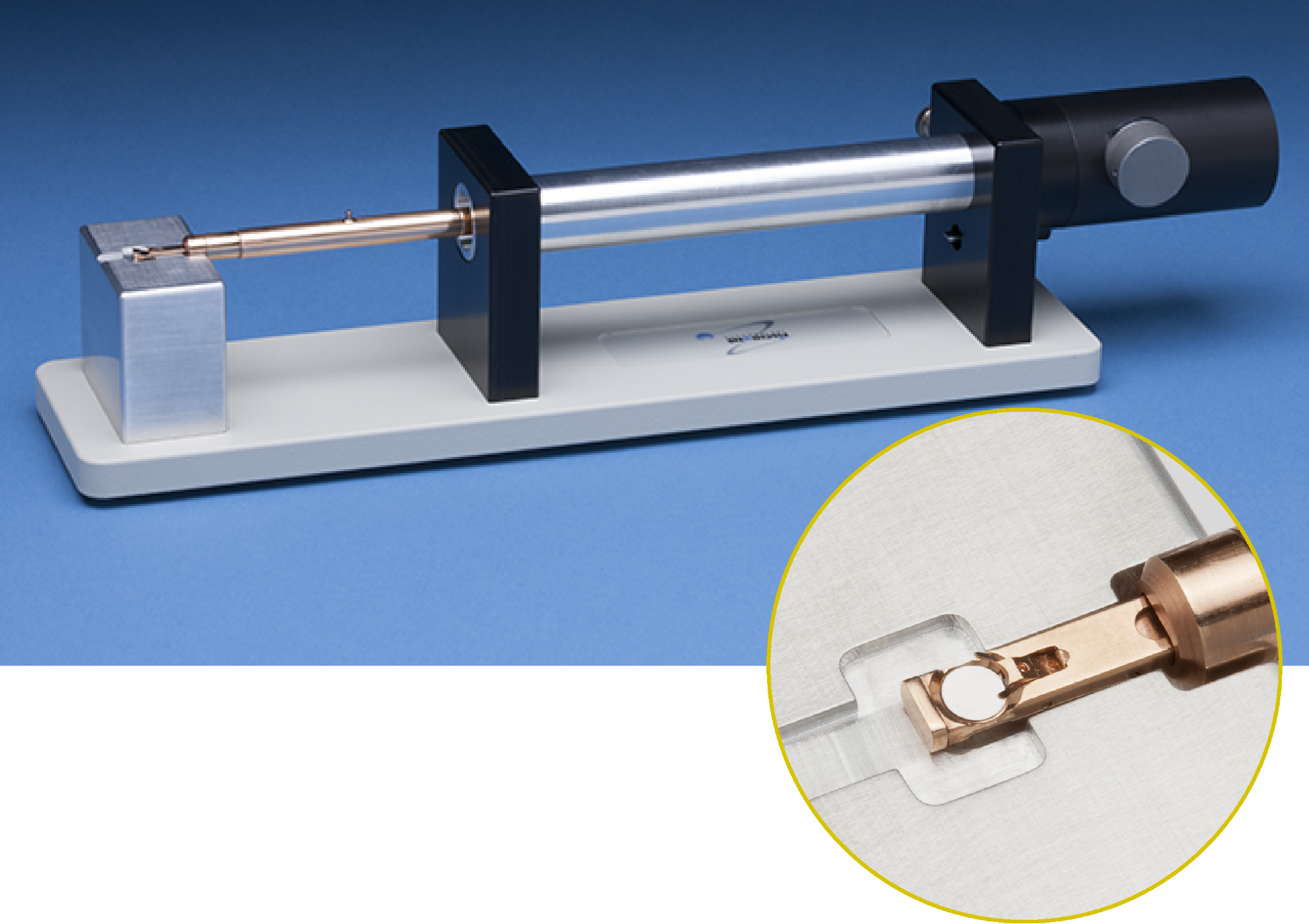
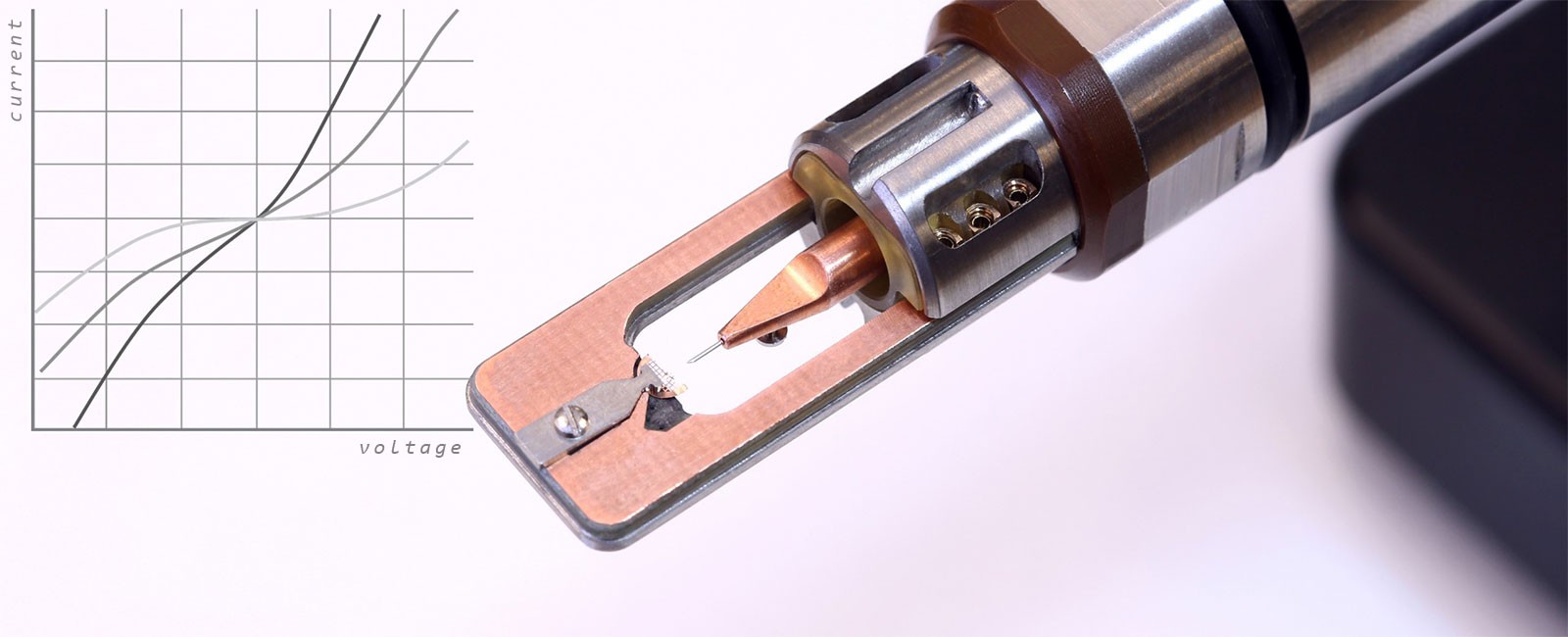
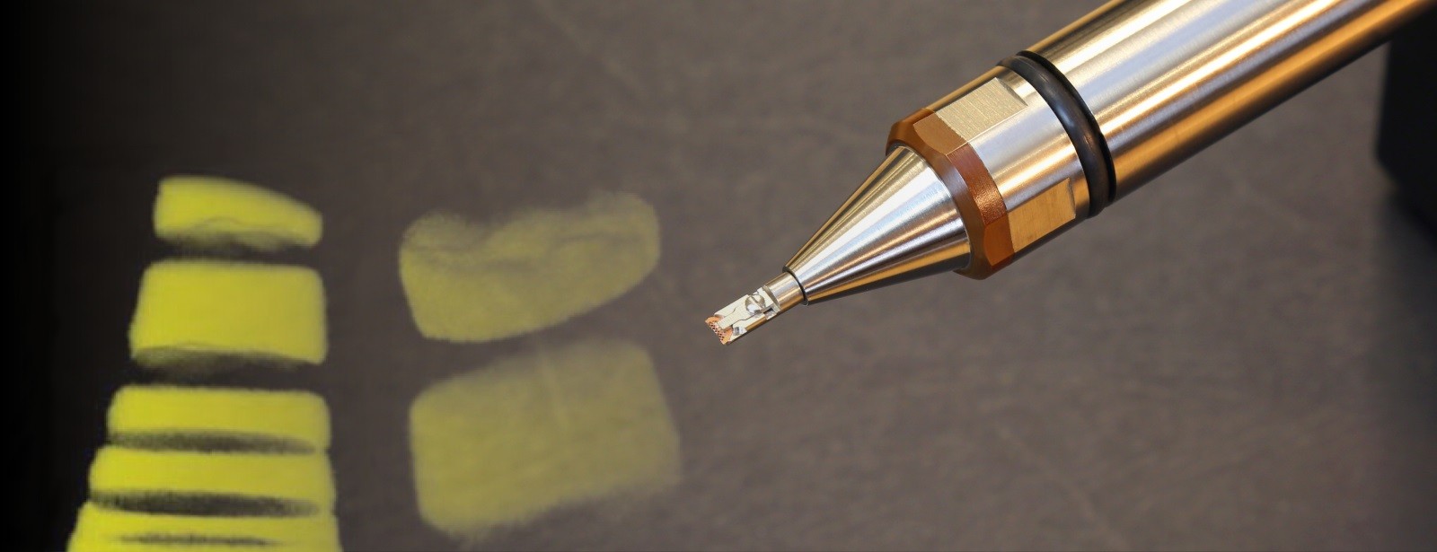
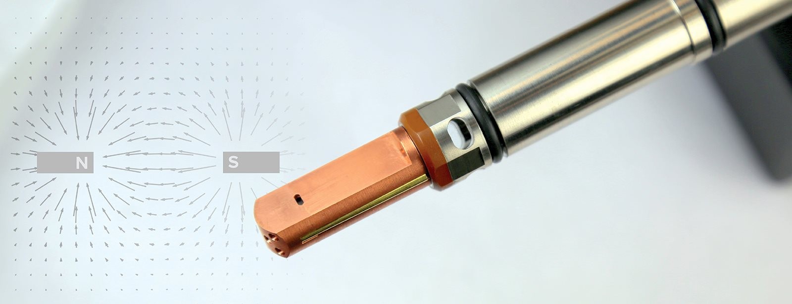
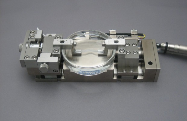
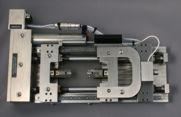
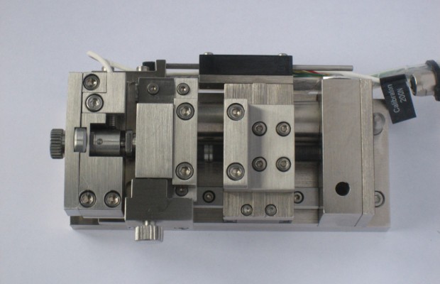
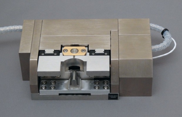
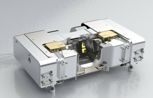
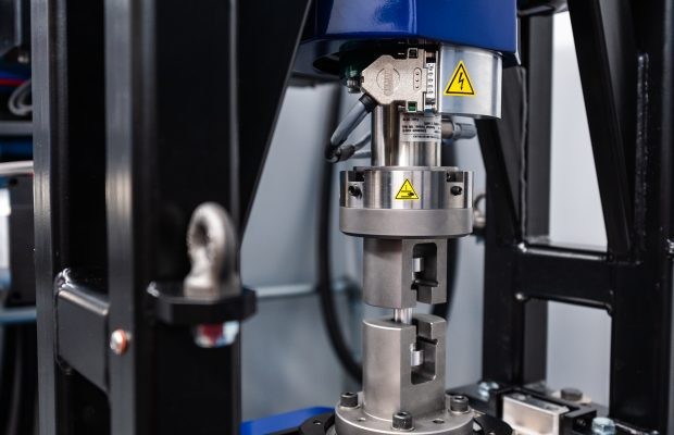
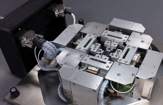
- The QUANTAX WDS (WDX) for SEM consists of the XSense wavelength dispersive spectrometer yielding the best resolution among all parallel-beam WDS systems. The large solid angle, due to the parallel-beam design, results in a much higher signal intensity for low-energy X-rays compared to a Rowland-circle based WDS spectrometer.
- The high signal-to-noise ratios that are characteristic for WDS are further enhanced by a unique secondary optic that suppresses background artefacts.
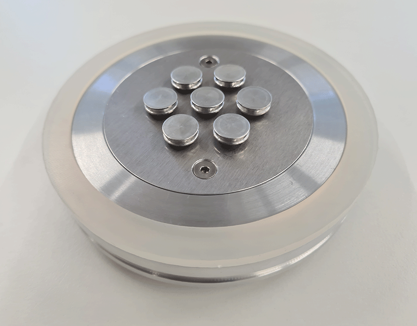
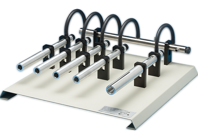
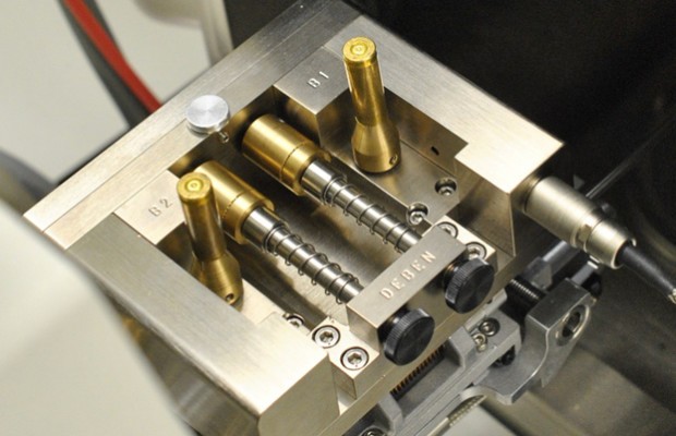
- Equipped with the finest grazing incidence optic and up to six analyzer crystals, the QUANTAX WDS has a superior sensitivity for low energy X-rays from 70 eV upwards.
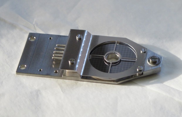
- An ingenious automatic optic alignment system and a unique pressure-controlled proportional counter ensure accurate and reproducible results.
- Flexible adaptation to either a WDS or EDS port.
WDS on SEM – a Perfect Solution for Demanding Analytical Applications
- Resolve common EDS peak overlaps such as Ta-W-Si, Pb-S, or Mo-S
- Explore low-energy X-ray line series (L, M, N) for the elements of interest
- Examine samples with low acceleration voltages to ensure a minimal depth of penetration
- Obtain the highest cps/nA due to the high solid angle that enables light elements investigation from Be to F across the entire concentration range
- Determine trace element concentrations far below the limits of detection of an EDS
- Measure at low vacuum without the necessity of a conductive coating
- Save time on analytical measurements with a unique pressure-controlled proportional counter
- Ensure spatial accuracy of the spectral data for precise quantification
- Save acquisition time with simultaneous WDS and EDS analysis that incorporates the benefits of each detector in the combined quantification
What is your Analytical Challenge?
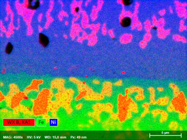
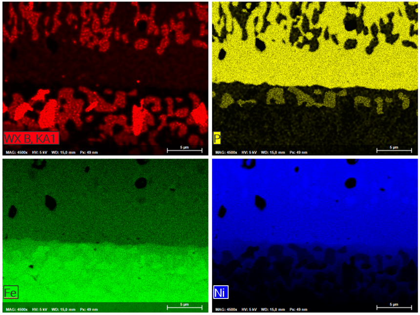
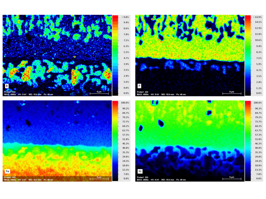
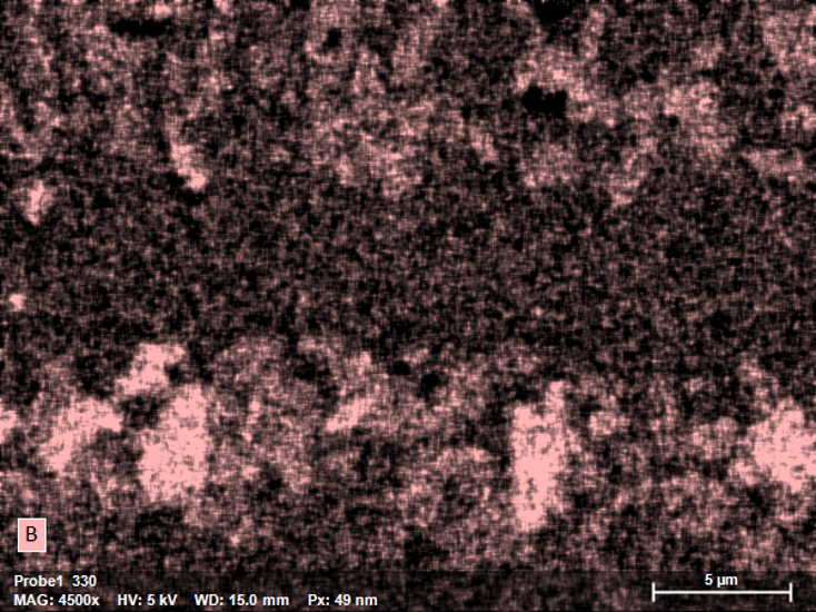
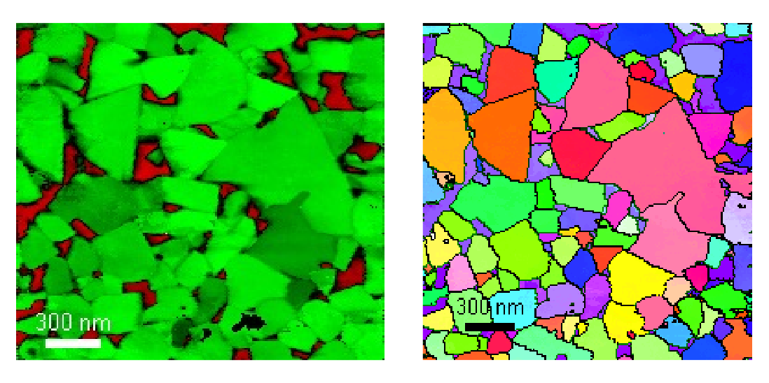
Elemental Mapping of a Dispersion Layer on Steel
Dispersion hardening can be applied to produce hard and wear-resistant surfaces for industrial tools and high-temperature materials. This type of precipitation hardening relies on non-metallic inclusions, such as borides, to block structurally weakening dislocations in the metal.
The analysis presented here shows a cross-section of the interface of a Ni-P-B dispersion layer on steel substrate 100Cr6. Element distribution maps from this sample derived by simultaneous WDS/EDS acquisition at 5kV, 16 nA characterize different boron precipitates in the dispersion layer and steel contact zone. Whereas single-type Ni-B-phases have segregated from the dispersion layer, three types of Fe-(Ni-, P-)borides have grown in the alteration zone of the steel substrate close to the contact with the dispersion layer.
Mapping the 30 x 22 µm area with a resolution of 600 x 450 pixels was accomplished in only 10 minutes using QUANTAX WDS with diffractor BRML200 for boron determination.
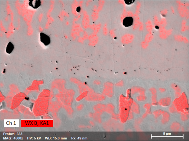
Comparison of the Boron Signal in EDS vs. WDS
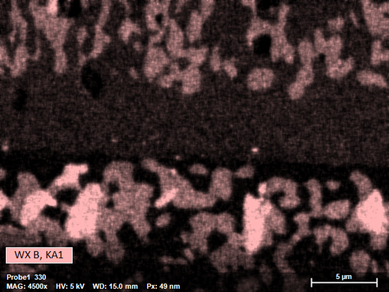
Thanks to its high sensitivity for low X-ray energies and improved counting statistics QUANTAX WDS can achieve better resolved map images. In this case acquisition time was only 5 minutes for both maps via simultaneous EDS and WDS acquisition.
QUANTAX WDS is a parallel-beam wavelength dispersive X-ray spectrometer optimized for the determination of low X-ray energies. With its grazing incidence optics, which capture X-rays close to the source or origin, and selected high efficiency multilayer diffractor elements for low energy X-rays, the QUANTAX WDS is much more sensitive to light elements than EDS. Compared to standard EDS (60 mm²), the signal intensity at 183 eV (B-Ka) is ca. 80 times higher with QUANTAX WDS, leading to fast and detailed mapping results.
Automated Phase Identification
QUANTAX WDS is fully integrated into Bruker’s ESPRIT software, making it easy to combine WDS and EDS datasets for joint mapping and data analysis. Add-on programs such as AutoPhase can be applied to the ESPRIT HyperMaps containing both WDS and EDS data, for users who wish to visualize chemically similar or different phases in their SEM samples.
AutoPhase is based on multicomponent analysis functions and converts the elemental distribution map into a phase map, which is the most intuitive way to visually distinguish phases with different compositions in a mapped sample. Another advantage of AutoPhase is the determination of the area fraction for each phase in the mapped image area.
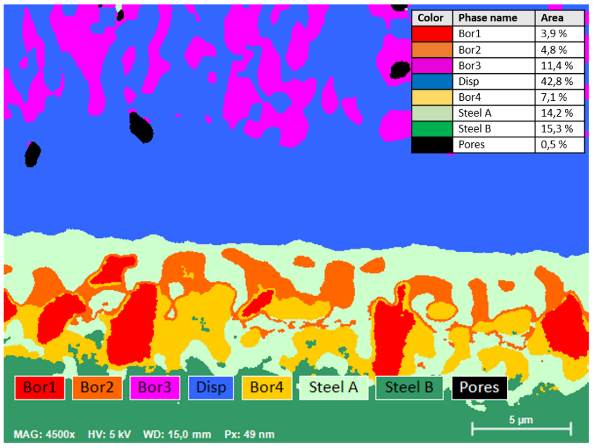
Phase map calculated from the WDS/EDS X-ray intensity map. Legend for phases: Bor1 = Fe-boride, Bor2 = P-rich Fe-Ni-boride, Bor3 = Ni-boride, Bor4 = P-poor Fe-Ni-boride, Disp = Ni-P-B dispersion layer, Steel A = overprinted Ni-rich steel, Steel B = original 100Cr6 steel. The table presents the area proportions of the different phases.
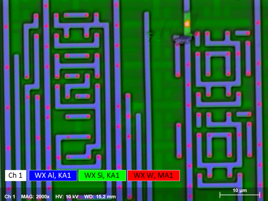
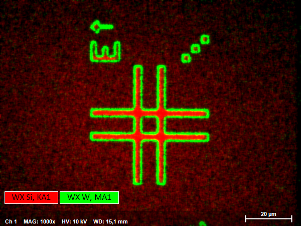
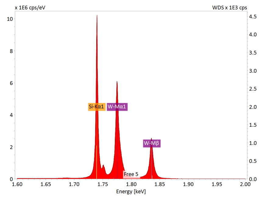
Elemental Identification in Semiconductor Microchips Materials
The electrically conductive ceramic material tungsten silicide is used in microelectronics such as microchips. Tungsten silicide may also occur as a refractory phase in semiconductor materials, such as Si wafers.
In order to achieve a high spatial resolution on the micro- and nano level during quality control, the analyses have to be carried out at low accelerating voltages, complicating the identification of these phases. Only the tungsten M series energy lines which severely overlap with the substrate Si Kα line are generated at low accelerating voltages.
The resulting EDS peaks of the primary elements are slightly broadened and masking the presence of the second phase. In contrast to that, elements such as W are identified with confidence using QUANTAX WDS due to its superior spectral resolution.
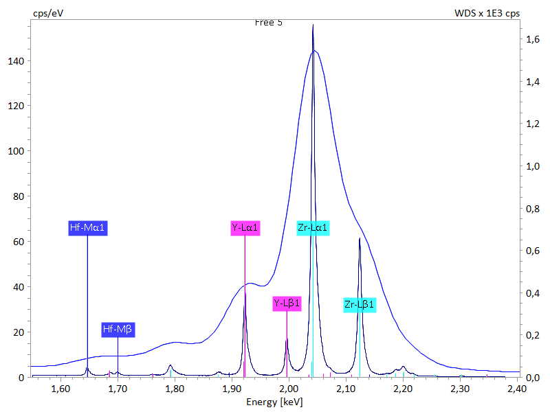
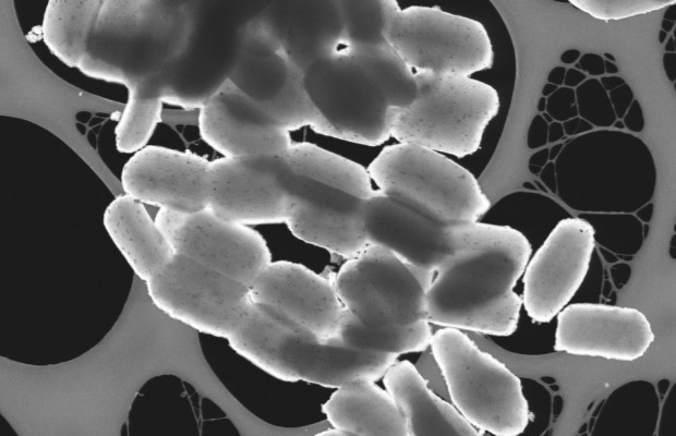
Gemstone Grading and Purity Control with WDS
Cubic zirconia (ZrO2) is a popular synthetic gemstone used as an economic substitute for diamonds in jewelry (Fig. 1). Calcium oxide (5–8 wt.%) or yttrium oxide (15–18 wt.%) are often added to stabilize the ZrO2 crystals. Moreover, other elements such as hafnium may also be present in minor amounts.
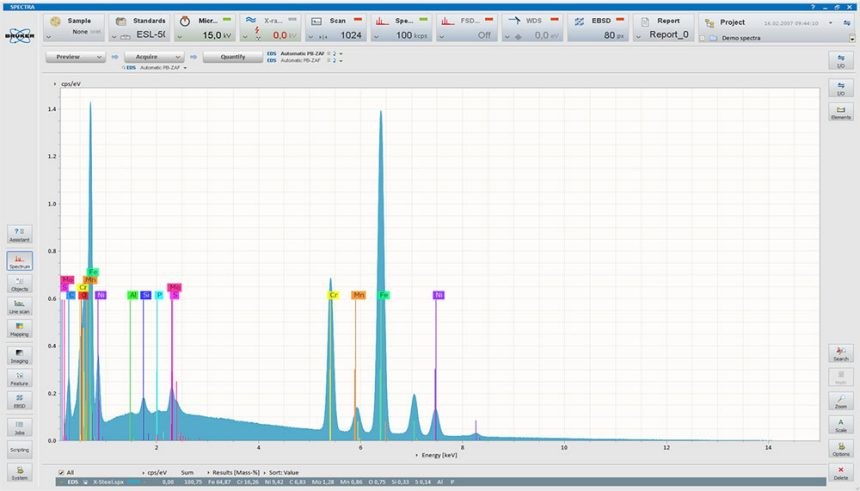
The EDS spectrum of a cubic zirconia (Fig. 2) shows a broadened, irregular Zr L peak but the contribution of other elemental lines cannot be distinguished easily. The WDS spectrum, in contrast, clearly resolves the various Zr L energy lines from the Y L energy lines and even detects Hf using M series energy lines. QUANTAX WDS with its high spectral resolution capability can thus be a valuable tool for gem grading and purity control.

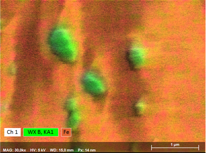
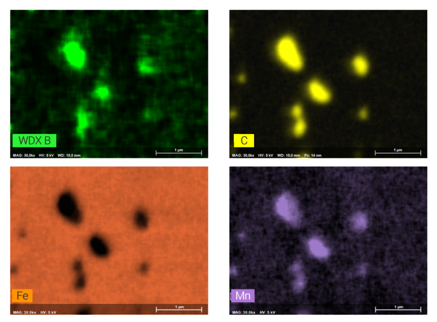
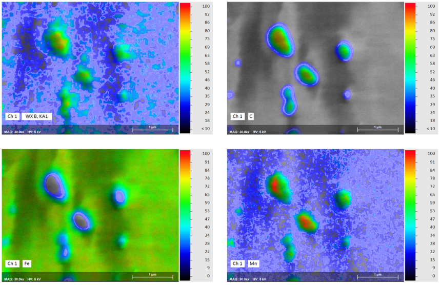
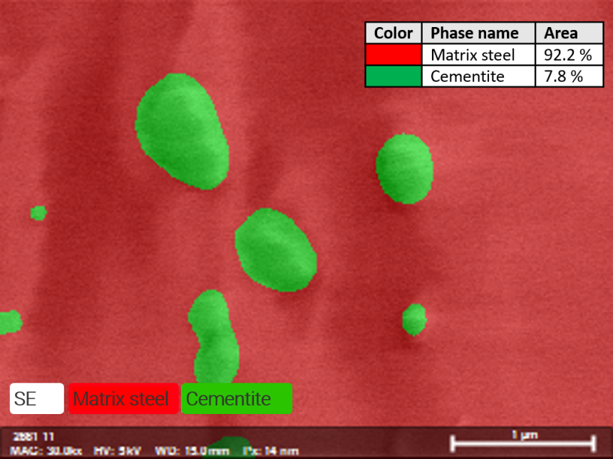
Elemental Mapping of Nanoscale Boron-Containing Phases in Steel
Boron is used in the steel industries as an alloying element in certain special steels: Boron-induced precipitation hardening can lead to the desired increase in yield strength and strength in some austenitic Cr-Ni-steels. Furthermore, the strength properties of high-temperature steel grades are improved at higher temperatures with the help of boron-induced precipitation. Steels alloyed with boron are also used in nuclear technology, as boron has a high effective cross-section for neutron absorption.
The example shown here of combined WDS/EDS mapping of a boron steel demonstrates that light element distributions can be mapped very well by QUANTAX WDS, even when concentrations are in the trace element range and phases of interest are extremely small.
The results show that relative boron enrichments are related to sub-micron size cementite phases (Fe3C) that are characterized by relative enrichment of carbon, manganese, chromium and boron. Boron contents in cementite determined by WDS are 0.4 wt% as compared to 0.2% in the steel matrix. Mapping the trace element distribution with a pixel resolution of 14 nm was done at 5 kV, 17 nA in 120 minutes using diffractor BRML200.
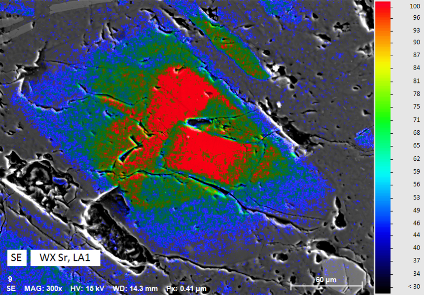
Mapping Trace Element Distribution in Plagioclase
Trace elements and their spatial distribution in rocks and minerals are of substantial interest to geoscientists; for example, in igneous rocks, trace elements are valuable tracers for magma sources and geological processes affecting the subsequent evolution of magma.
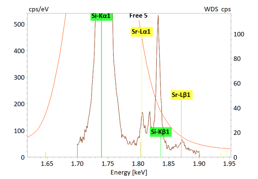
The present map shows the distribution of strontium (Sr) in a plagioclase (sodium-calcium feldspar). Sr is a trace element in plagioclases and of special interest since it can be used for diffusion chronometry or for studies of crystal-melt evolution. The analytical challenge in this case is not only related to the low concentration of the element of interest (Sr < 1000 ppm), but also to the distinct EDS peak overlap of Si Kα and Sr Lα.
QUANTAX WDS is perfectly suited for mapping and in-situ analyses of trace elements in minerals. The WDS technique is indispensable especially under such analytical circumstances where the close proximity of X-ray lines coincides with pronounced differences in line intensities.
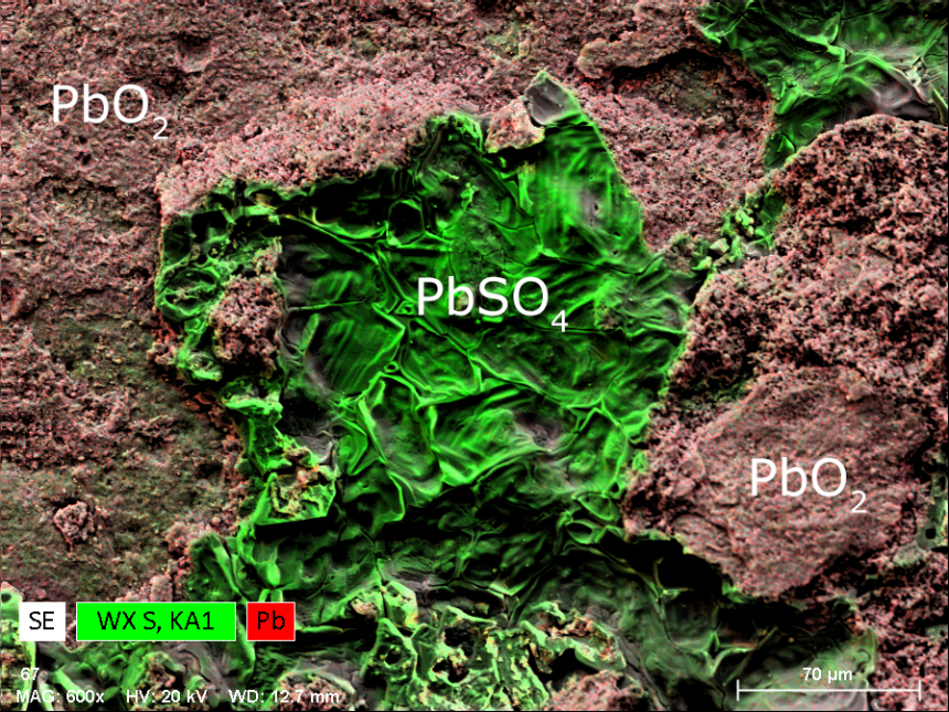
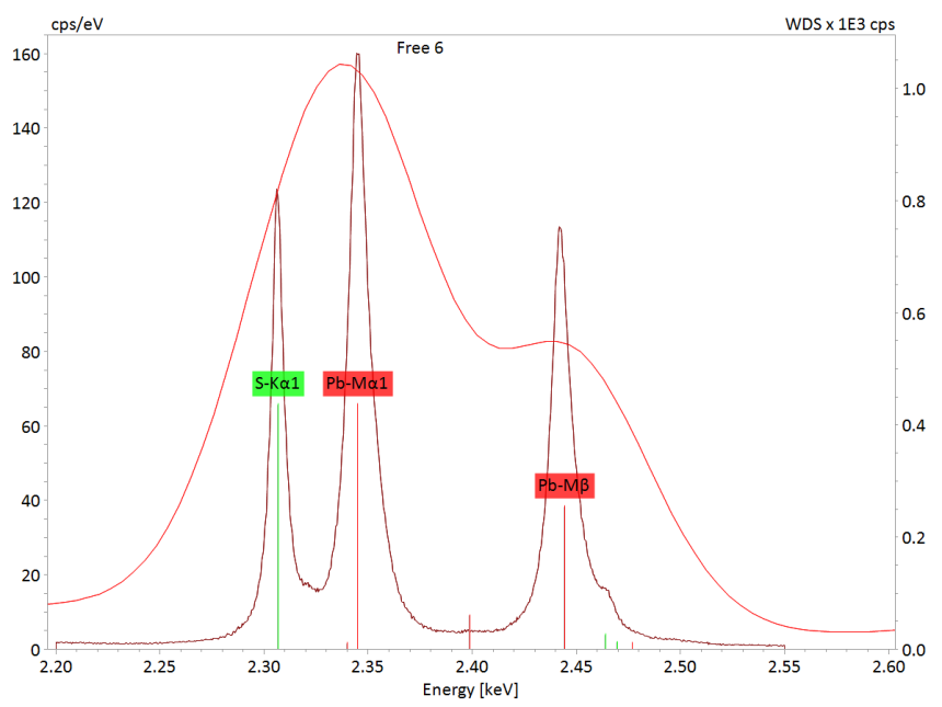
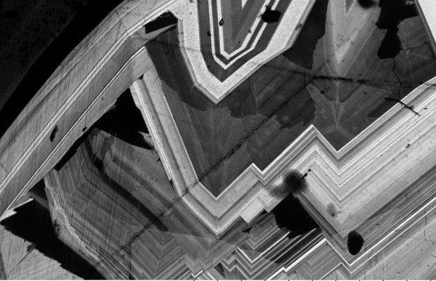
Sulfate Alteration of Lead Acid Batteries
Lead-acid batteries (accumulators) are rechargeable devices for storing electric energy generated by electrochemical processes. The batteries consist of electrodes made of lead (Pb) and lead dioxide (PbO2) and dilute sulfuric acid (37% H2SO4) as electrolyte.
During discharge of lead-acid batteries, finely dispersed lead sulfate (PbSO4) forms on electrodes in a process that is reversed by recharging. However, sulfation, a permanent alteration process characterized by the formation of coarse crystalline lead sulfate deposits, may lead to progressive inhibition and power loss of the battery until complete failure upon short-circuit. The nature, kinetics and spatial distribution of these crystalline deposits is thus of major research interest for battery manufacturers as well as for developers of technologies preventing sulfation. X-ray element maps are ideal for investigating the nature and spatial distribution of sulfation deposits.
QUANTAX WDS is a powerful analytical tool which can well resolve X-ray overlaps of Pb and S and therefor determine the nature and spatial distribution of chemical phases generated during battery alteration.
-
-
-
-
-
-
-
-

-
-
-
-
-
-

-
-
-
-
-
-
-
-

-
-

-

-

-

-

-
-
-

-
-
-
-
-
-
-
-
-
-
-
-
-
-
-
-
-
-
-
-
-
-
-
-
-
-
-
-
-
-
-

-
-
-
-
-
-
-
-
-
-
-
-

-
-
-
-
-
-
-
-
-
-
-

-
-
-

-
-

-
-
-

-
-

-
-
-
-
-
-
-
-
-
-

-
-
-

-