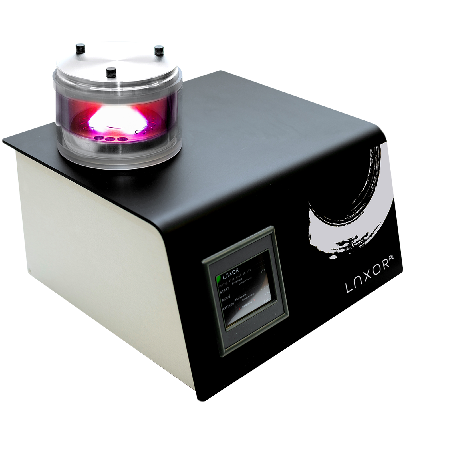
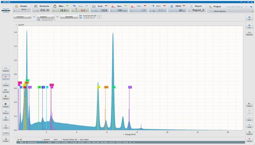
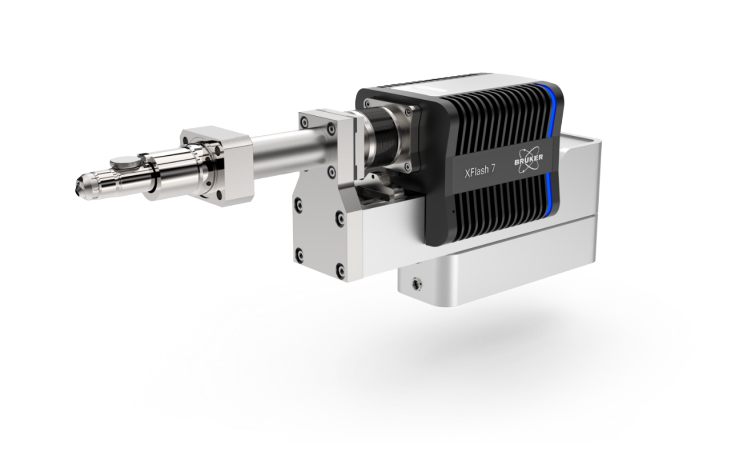
QUANTAX EDS for SEM
The Right Angle for Better Analysis Fast. Precise. Reliable.
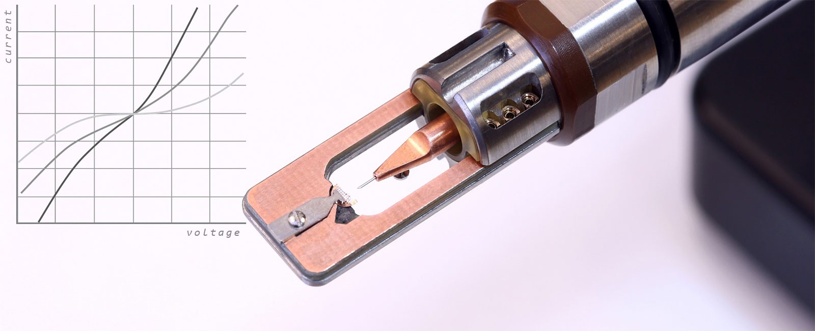
1,000,000 cps
Real analytical throughput up to 1,000,000 cps
Achieve unmatched analysis speed
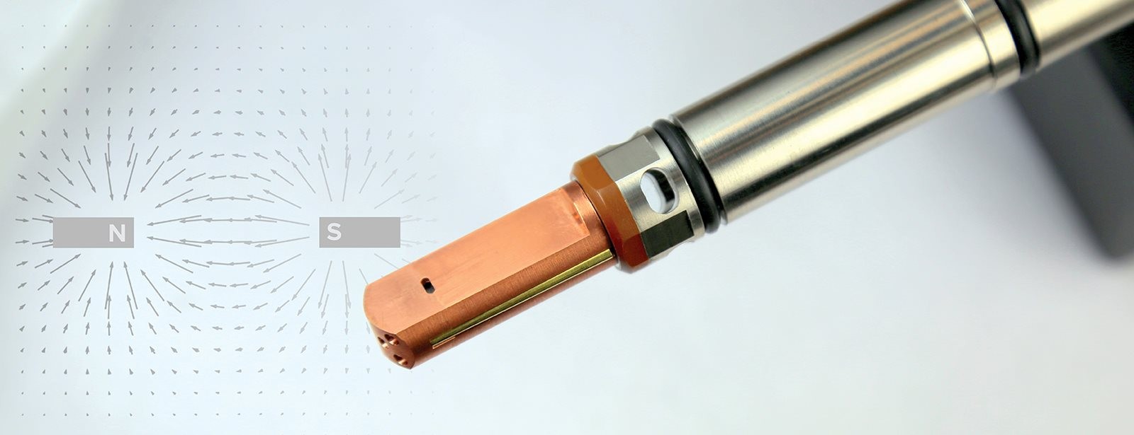
> 1.1 sr
Largest solid angle for X-ray collection
Maximize your sample throughput with optimum geometry for most efficient collection of the generated X-rays
https://youtu.be/laycUS1BesI
Make Your Elemental Analysis more Efficient!
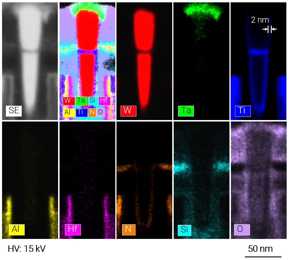
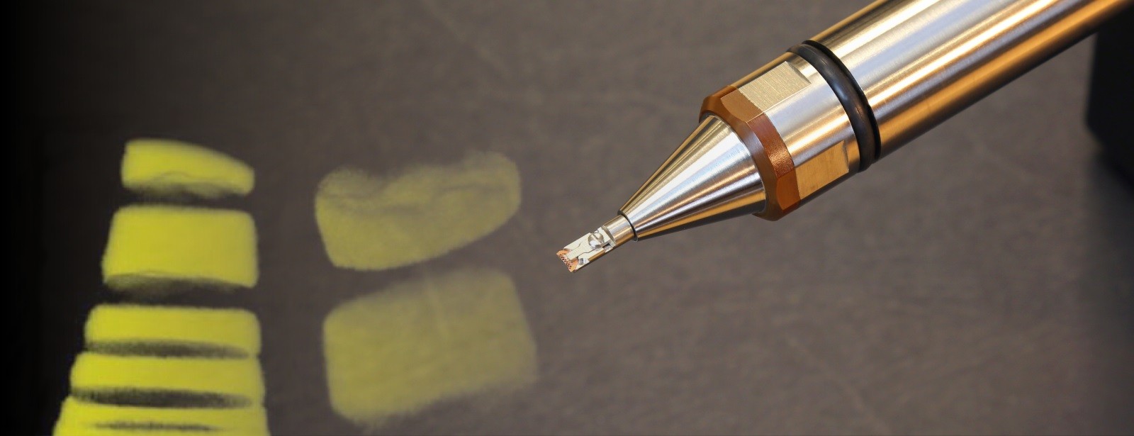
> 2,200 Element lines
Quantify the most complex data using the most comprehensive atomic database incl. K, L, M and N lines
For more details: Bruker EDS
For more details: Bruker EDS
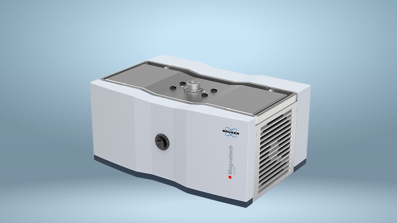
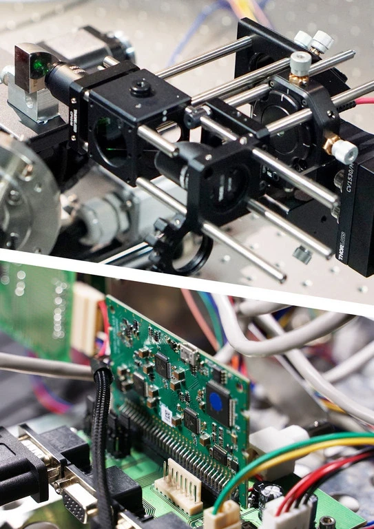
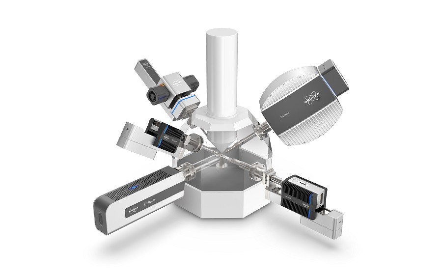
Energy-Dispersive Spectrometry for SEM, FIB-SEM and EPMA
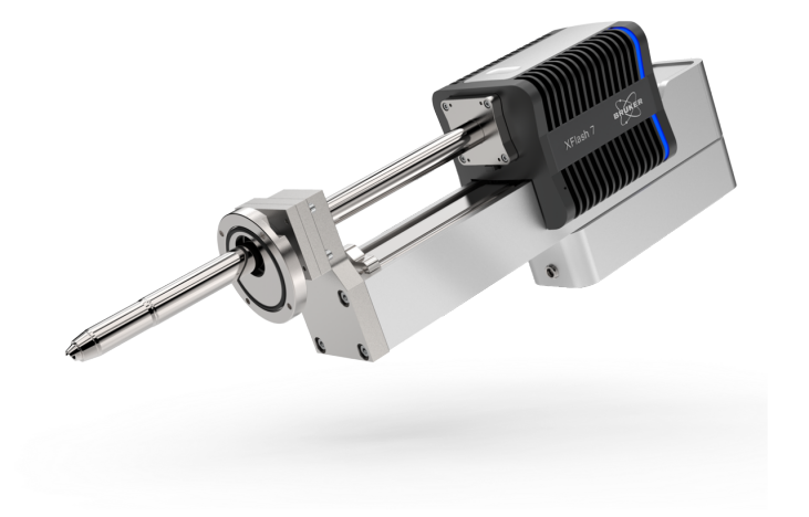
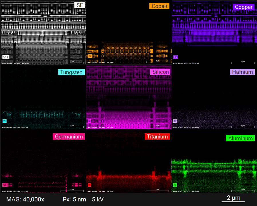
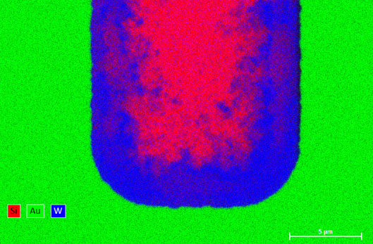
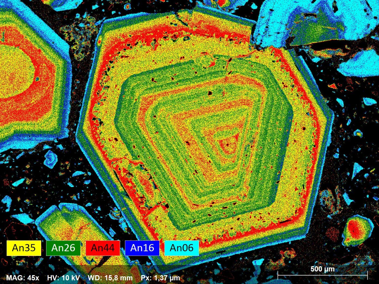
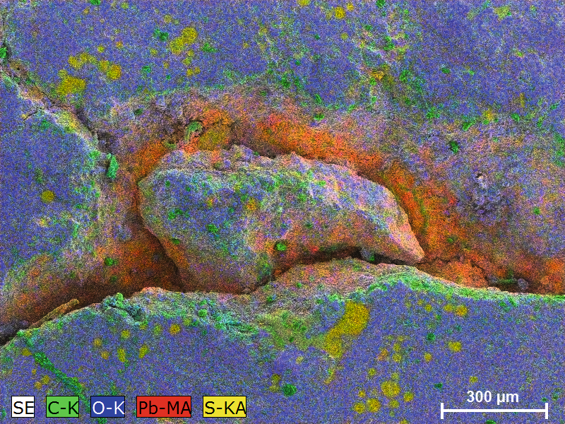
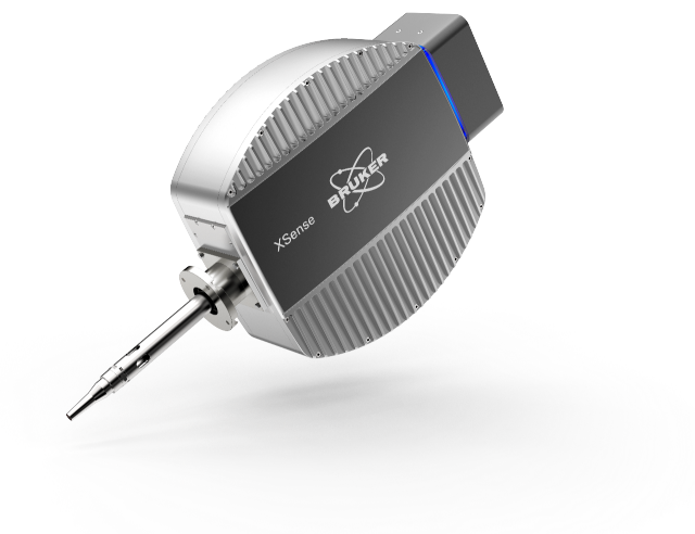
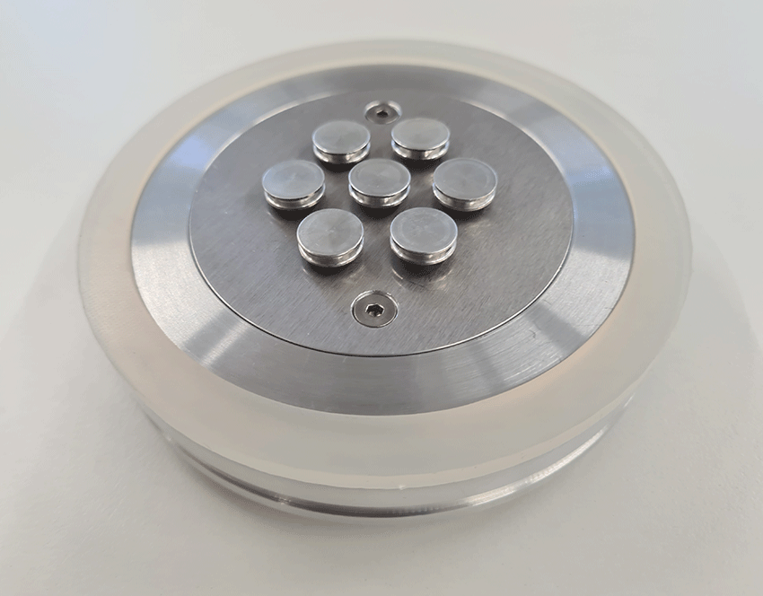
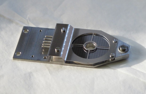
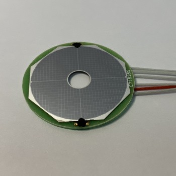
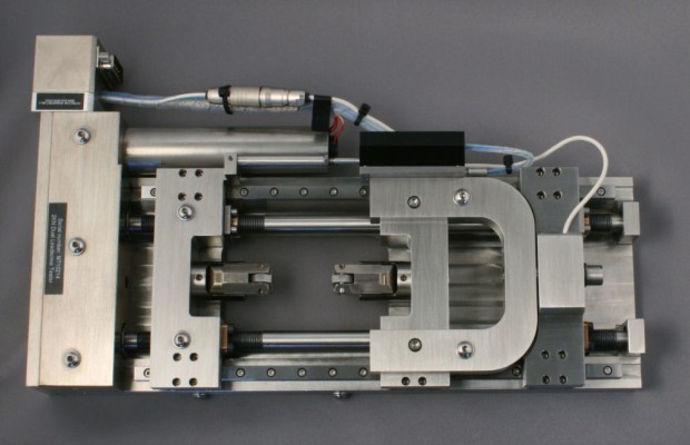
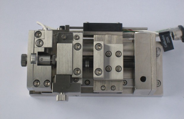
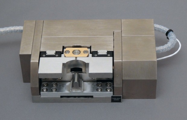
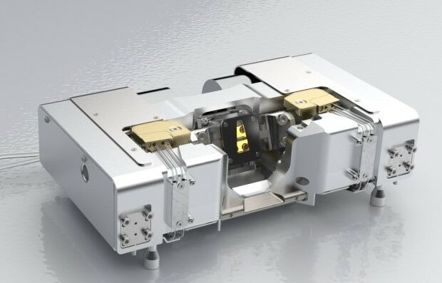
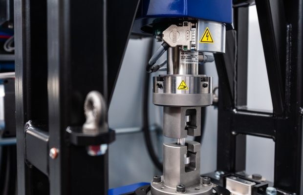
- Bruker's latest generation of QUANTAX EDS features the XFlash® 7 detector series, which provides the largest solid angle for X-ray collection (also called collection angle) and the highest throughput.
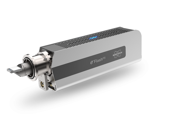
- The XFlash® 7 continues to set standards in performance and functionality in energy-dispersive spectrometry for the Scanning Electron Microscope (SEM), Focused Ion Beam (FIB-SEM) and Electron Probe Micro Analyzer (EPMA).
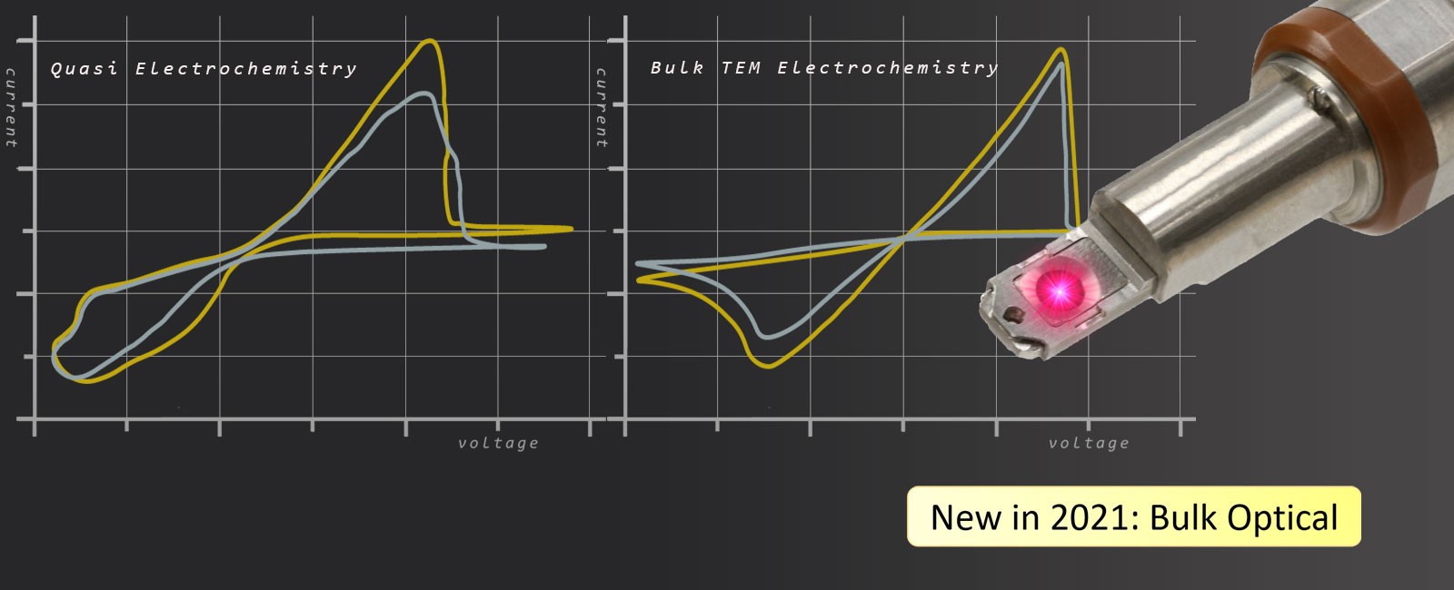
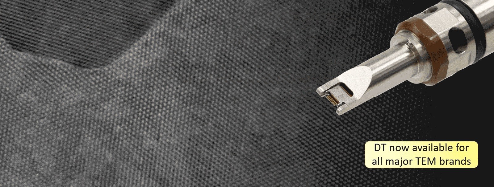
- The XFlash® 7 detector family also offers optimized solutions for EDS analysis of electron transparent specimens in TEM and SEM, as well as the unique XFlash® FlatQUAD, a detector made to answer your questions on challenging samples.
- Slim-line technology, large collection angle design and latest generation pulse processing.
- Increase system uptime with on-site SDD module exchange.
- Highest spectral performance obtained with best energy resolution.
- Increased accuracy of results by sophisticated quantification algorithms and a unique combination of standardless and standard-based methods.
https://youtu.be/laycUS1BesI
Make Your Elemental Analysis more Efficient!

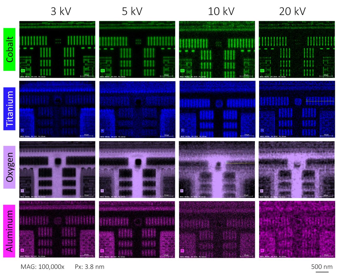
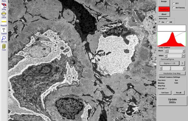
- Gain very precise results faster with individually optimized EDS systems. It ensures unmatched speed and precision.
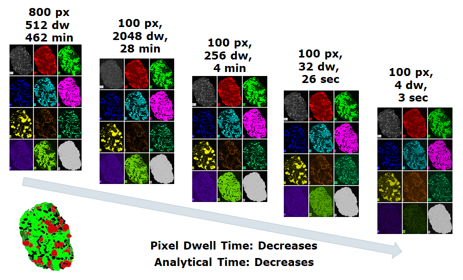
- Shorten measurement time with maximized throughput, enabling mapping and quantification at all settings with no limitation of data size.
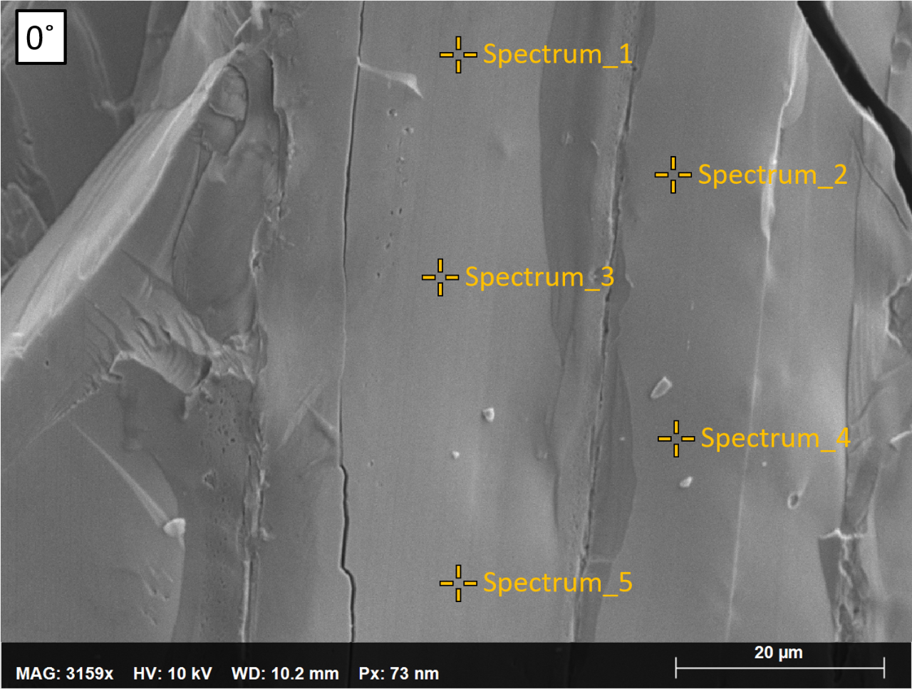
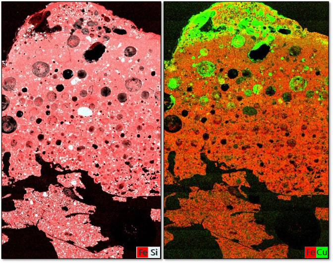
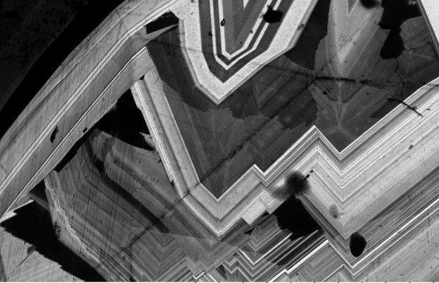
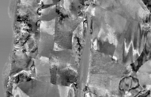
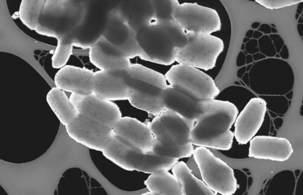
- Analyze challenging samples now, thanks to the most efficient geometric collection of generated X-rays.
- Benefit from accurate and reliable quantification results with optimized geometry minimizing background and avoiding absorption.
- Detect small quantities with better detection limit, lower background and less absorption.
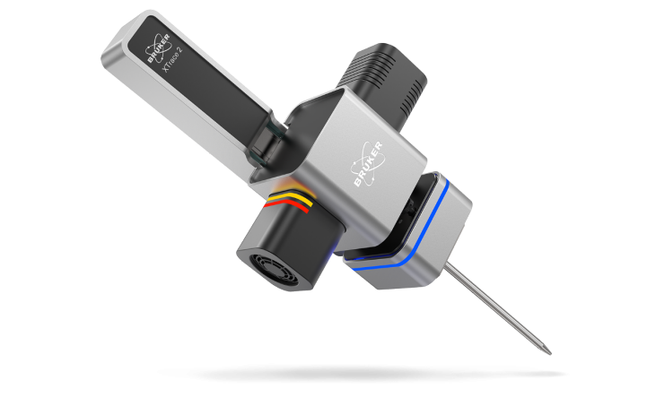
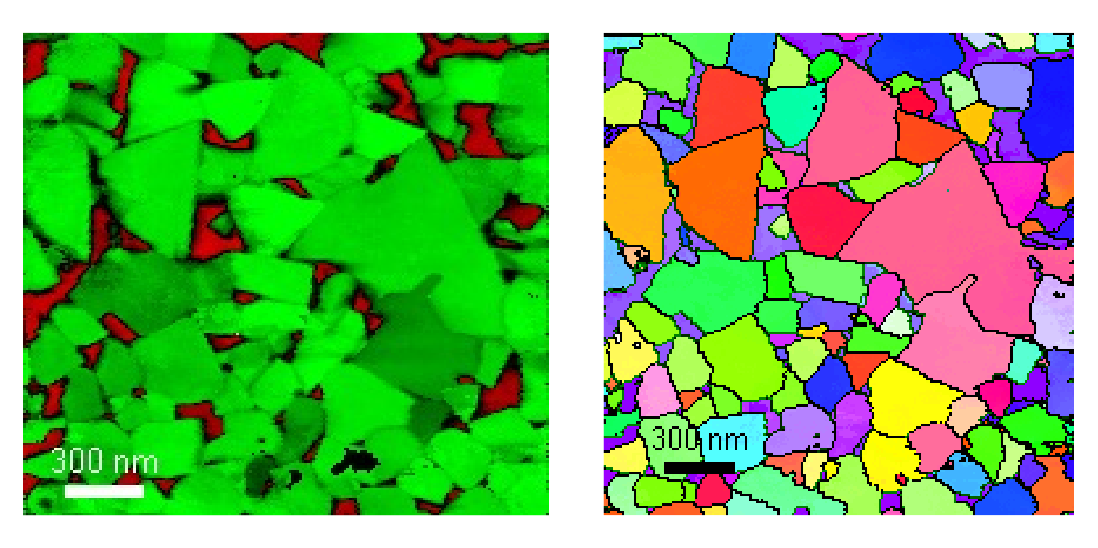
- One for all - seamless integration of EDS, WDS, EBSD, and Micro-XRF in the comprehensive ESPRIT analysis platform for any SEM, FIB-SEM and EPMA.
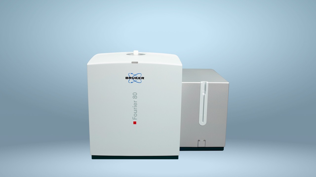
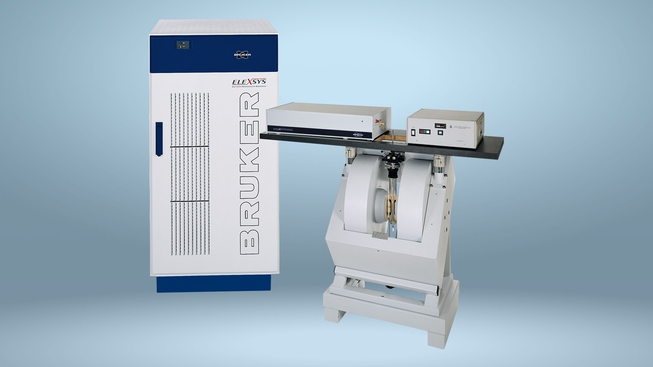
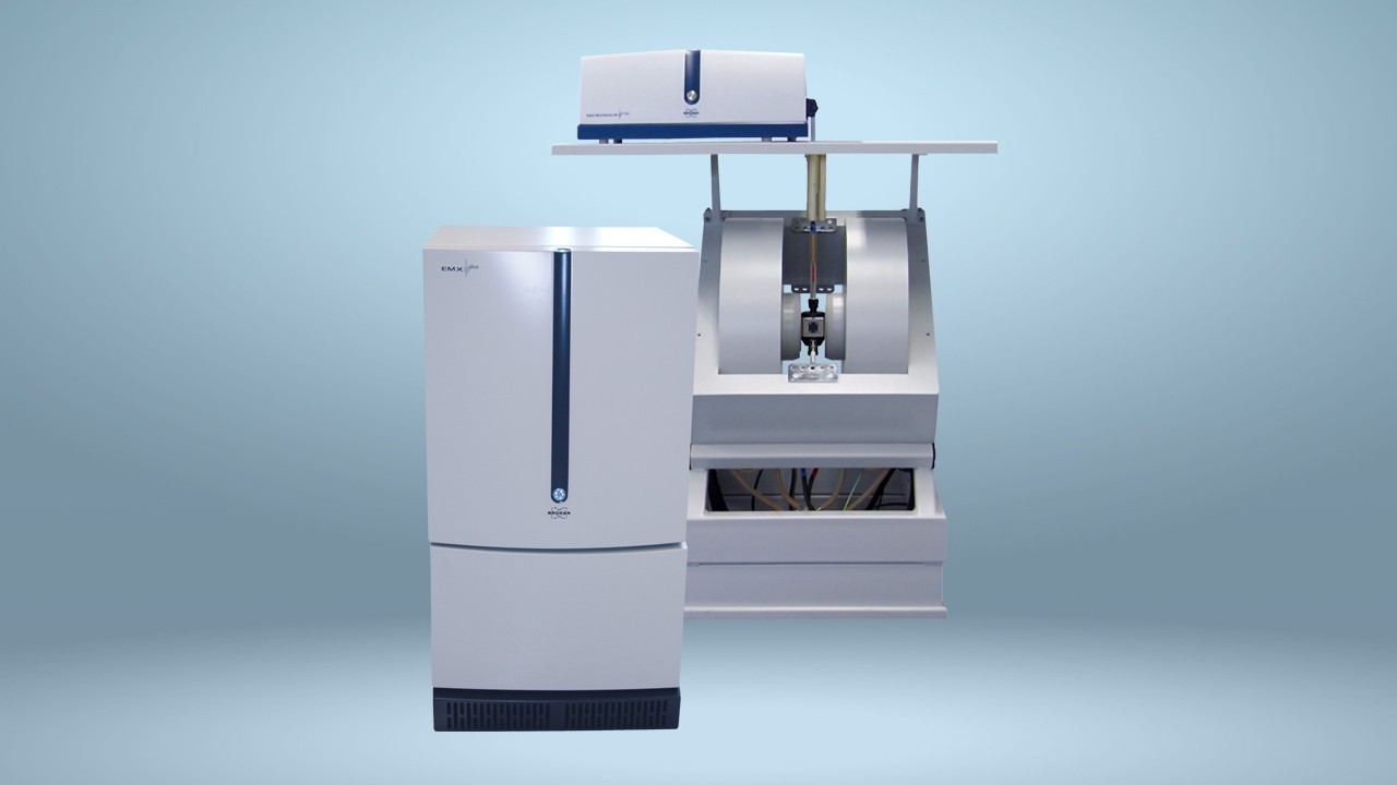
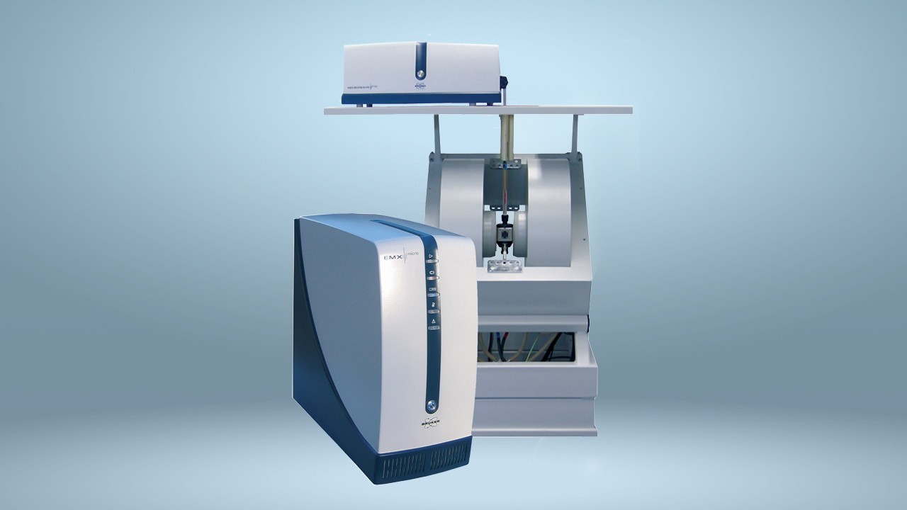
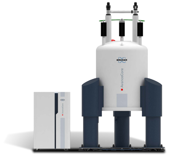
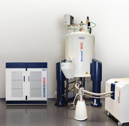
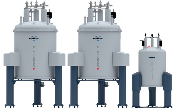
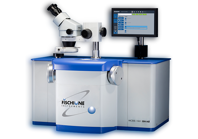
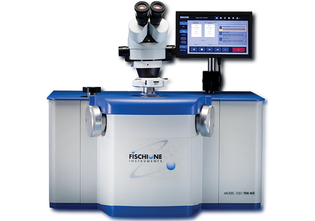
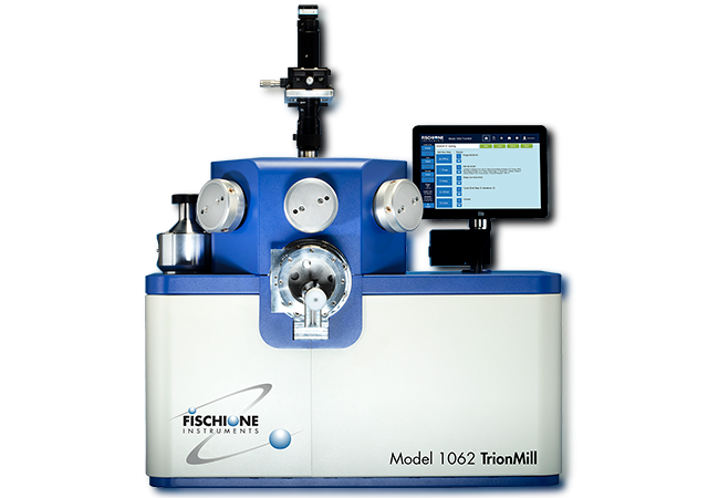
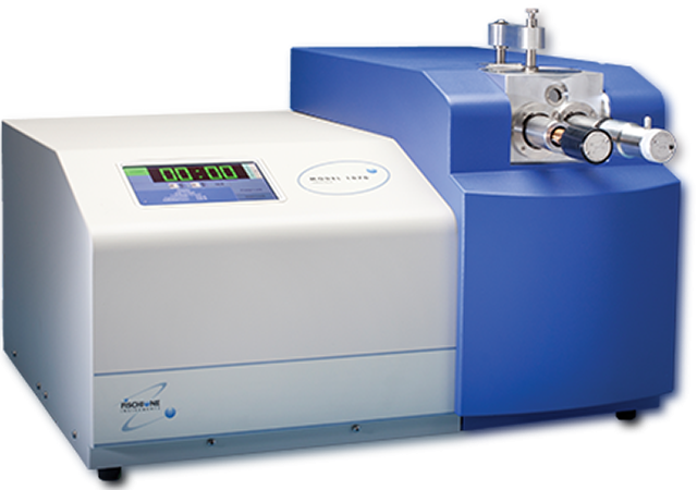
Diğer Ürünler
-
-
-
-
-
-
-
-

-
-
-
-
-
-

-
-
-
-
-
-
-
-
-
-

-

-

-

-

-
-
-

-
-
-
-
-
-
-
-
-
-
-
-
-
-
-
-
-
-
-
-
-
-
-
-
-
-
-
-
-
-
-

-
-
-
-
-
-
-
-
-
-
-
-

-
-
-
-
-
-
-
-
-
-
-

-
-
-

-
-

-
-
-

-
-

-
-
-
-
-
-
-
-
-
-

-
-
-
-