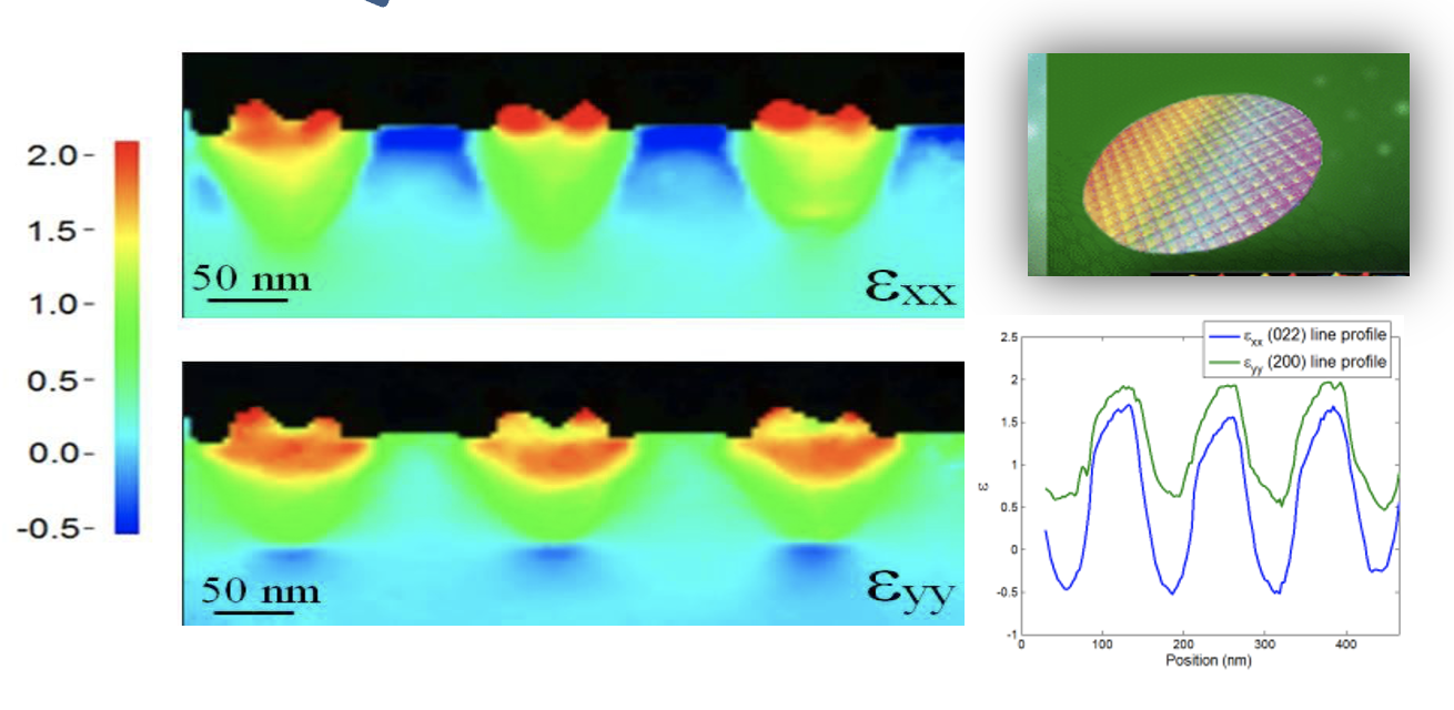
Strain mapping analysis
In modern transistor devices strain monitoring is critical for process development. Strain metrology on these devices demand a high degree of accuracy, precision and efficiency in data acquisition. At the scale of these devices, strain measurement using transmission electron microscope (TEM) is the only approach that can provide the adequate spatial resolution.
Existing TEM methods to measure strain include convergent beam electron diffraction (CBED), dark field electron holography, high resolution imaging and nanobeam diffraction (NBD). Although CBED is an accurate way to measure strain, the sample needs to be relatively thick (>150 nm) which limits its applicability to semiconductor devices. Dark field holography is another attractive approach although the experimental difficulties limits its application as a strain metrology technique. High resolution imaging offers the best spatial resolution for strain measurement. However, the sample needs to be ultra thin with uniform thickness and no bending. This stringent requirement along with limited field of view makes it difficult to use high resolution imaging for routine strain analysis.
Of these techniques, NBD is the most practical approach with good spatial resolution and ease of implementation. Hence NBD has been adopted widely in the industry for strain metrology. Strain measurement using NBD involves measurement of shift in individual diffraction spots. However, the presence of strong dynamical effects in electron diffraction is a serious limitation to achieve the desired precision. Since strain is measured using NBD patterns that are exactly on zone axis, the dynamical effects are exacerbated. Because of the dynamical effects, spot intensity distributions are strongly dependent on local specimen thickness and orientation.
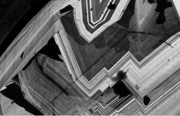
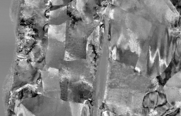
Although the technique is straightforward, it requires tedious specimen tilting to align specimen exactly at the zone axis. Figure below compares two Si diffraction patterns from near by regions in the same specimen prepared by focused ion beam milling.


(Left) Si <110> Diffraction patterns from two nearby regions in a FIB sample. Note the strong intensity variations due to dynamical effects.(Right)Si <110> Diffraction patterns from the same region as shown in Fig. 1 with 1∘precession.
Topspin strain analysis is a novel approach to strain measurement that combines NBD with precession electron diffraction to overcome the above mentioned limitations. Further, Topspin strain analysis uses a robust analysis algorithm for high accuracy and precision with the ability to handle overlapping patterns.
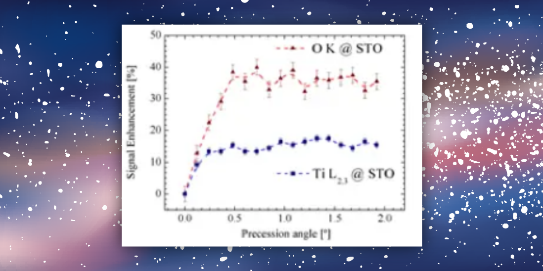
Precession offers the following advantages for strain measurement:
-Dynamical effects are reduced even when the specimen is close to zone axis. Because of this diffraction patterns are less sensitive to changes in thickness
-The use of precession also enables the collection of higher order reflections which are more sensitive to small variations in strain
-Zone axis alignment is easier with precession as the averaging of diffraction patterns over different tilts results in a symmetric diffraction pattern even when the specimen is slightly off axis.
-Effect of specimen bending is mitigated with precession.
Topspin strain analysis uses a proprietary algorithm to identify all the spots from the crystal of interest with the desired orientation. For most Si devices, this is the <110> zone axis pattern of Si. The algorithm uses a model based approach to accurately find the spot positions for both thereference and the strain diffraction patterns.
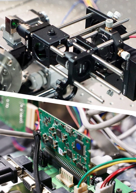
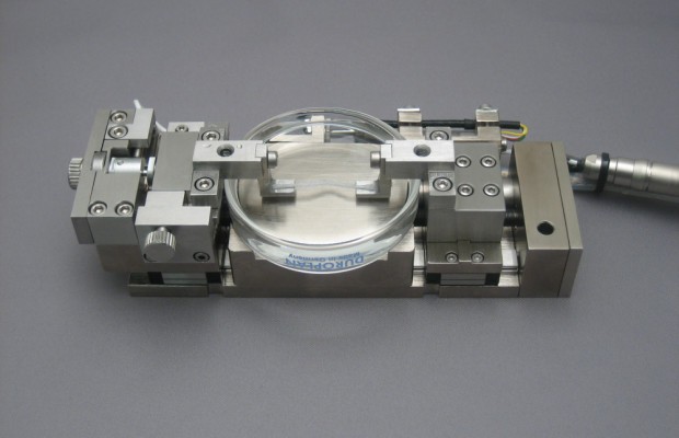
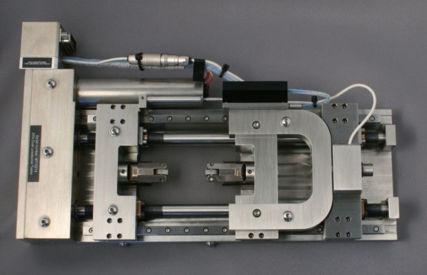
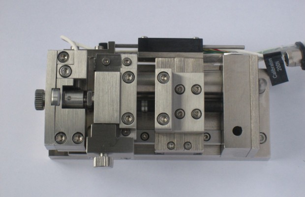
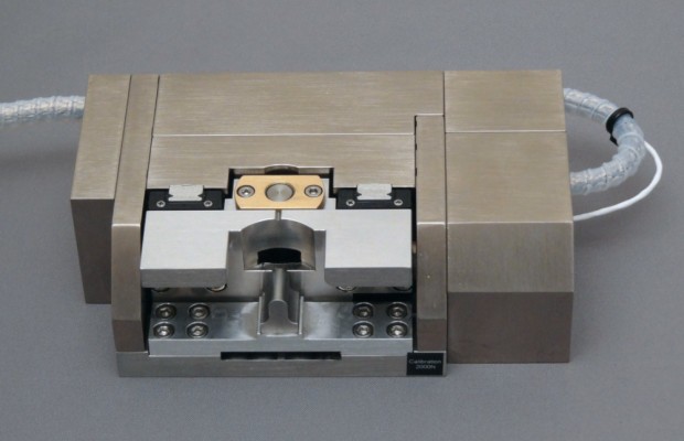
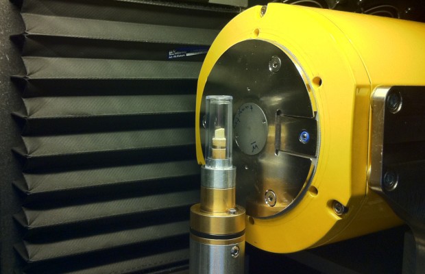
Topspin hardware consists of Digistar , which enables synchronized beam scanning with precession. Topspin system can be installed on most modern microscopes and it does not require a scanning unit to be present on the microscope. Topspin has a streamlined workflow which makes it possible to acquire strain data sets with minimal time for set up. In a typical Topspin set up typical precession angle is of 1∘, acquisition time for 150 x 150 map is 5-10 min, typical strain analysis time is 5 to 10 min.
-
-
-
-
-
-
-
-
-

-
-
-
-
-

-
-

-
-
-
-
-
-
-
-

-

-
-

-
-
-
-

-
-
-
-
-
-
-
-
-
-
-
-
-
-
-
-
-
-
-
-
-
-
-
-
-
-
-
-
-
-
-

-
-
-
-
-
-
-
-
-
-
-
-

-
-

-
-
-
-
-
-
-
-
-

-
-
-

-
-

-
-
-

-
-

-
-
-
-
-
-
-
-
-
-

-
-
-

-