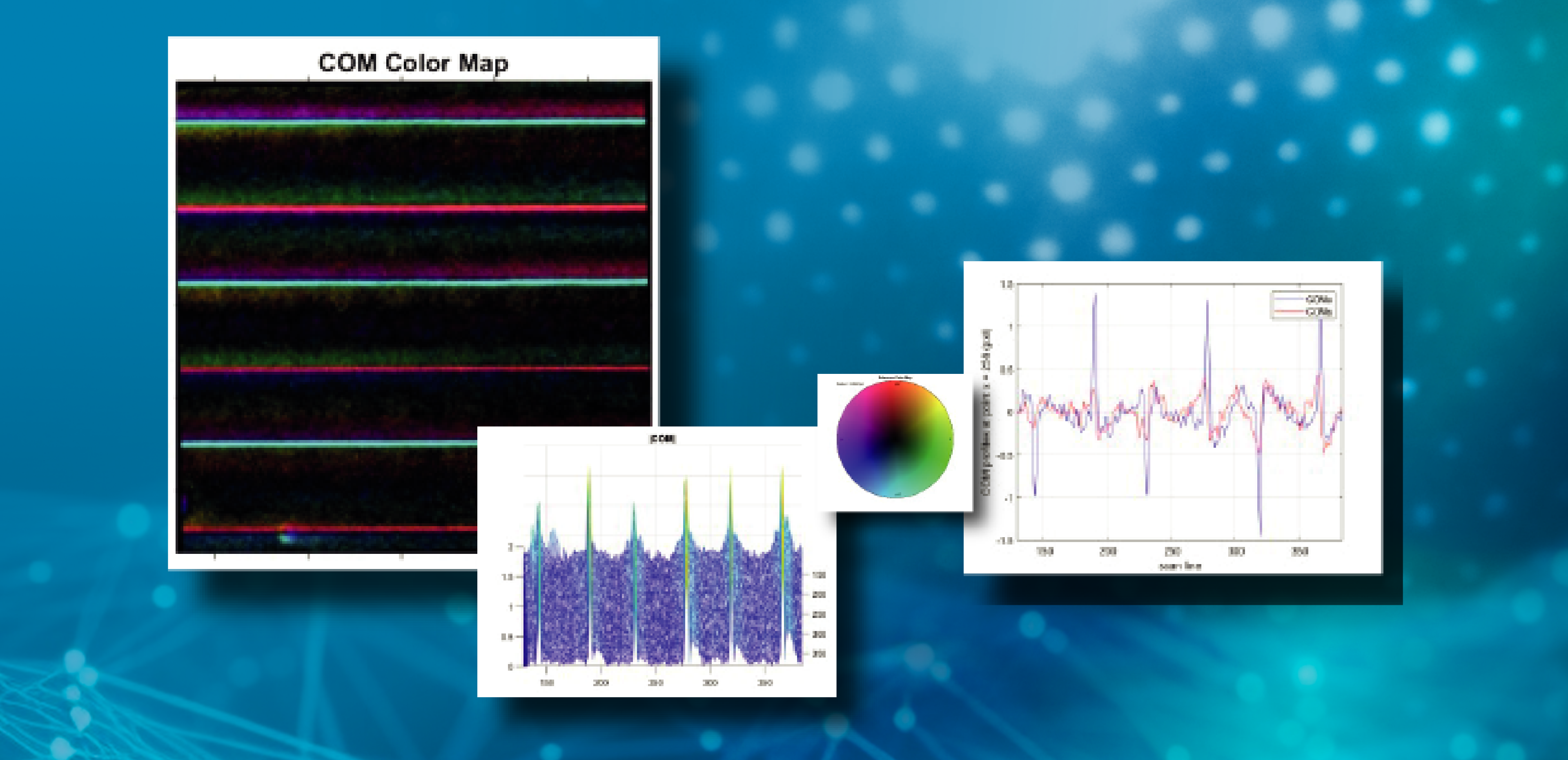
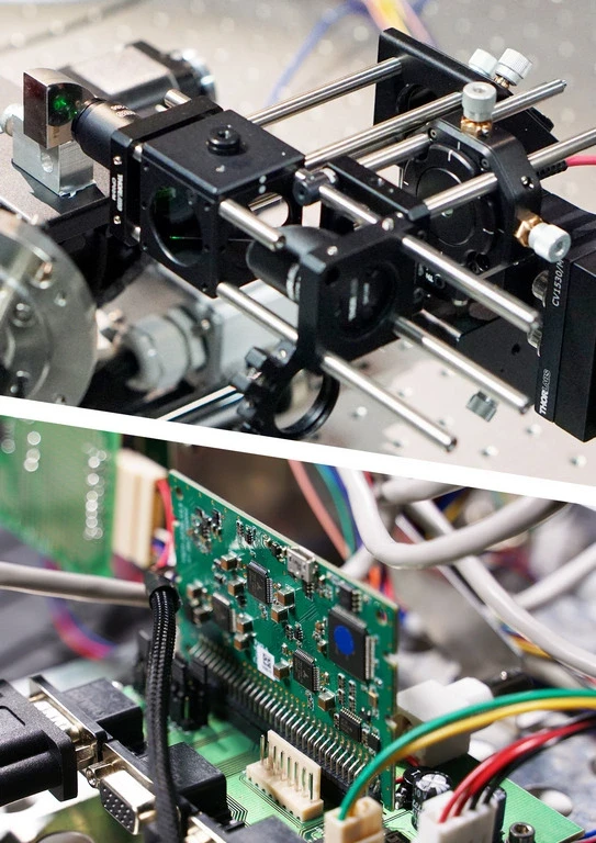
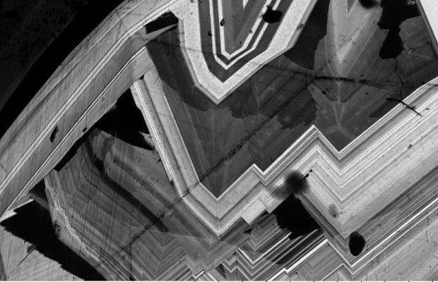
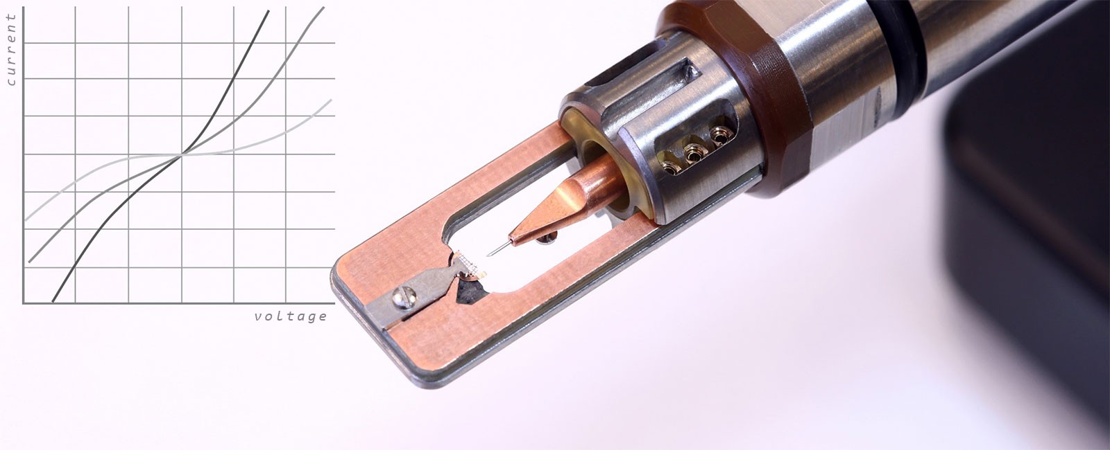
4D-Scanning Precession Electron Diffraction (4D-SPED) acquisition method in TEM, is currently used in several applications for materials analysis like Orientation & Phase mapping and Strain analysis [1]. 4DSPED is an extension of 4D-STEM technique and it consists in scanning the electron beam over the structure to observe and record at each position a Precession Electron Diffraction Pattern (PED) pattern.
4D-SPED acquisition together with data processing dedicated software is applied to characterize in detail local electric/magnetic fields and built-in potentials in functional materials.
During scanning over the sample, the transmitted beam is deflected though the local electric field by the Lorentz force.
The module of the local electric field translates into the shift of the intensity distribution in the transmitted central electron beam.
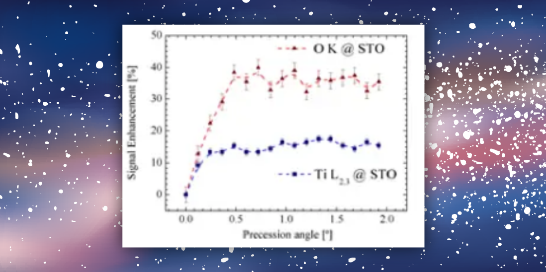
Electric filed is relying on COM (center of mass) displacement of the illumination intensity. Beam Precession of 0.1-0.4 degrees is used to get rid of dynamical effects and obtain ED patterns with less noise leading to enhanced results. Electric field calculations are of high interest to study properties of many materials and devices, e.g. transistors, solar cells or sensors, nanowires, batteries, etc.
-
-
-
-
-
-
-
-
-

-
-
-
-
-
-

-
-

-
-
-
-
-
-
-

-

-

-

-

-
-
-

-
-
-
-
-
-
-
-
-
-
-
-
-
-
-
-
-
-
-
-
-
-
-
-
-
-
-
-
-
-
-

-
-
-
-
-
-
-
-
-
-
-
-

-
-
-
-
-
-

-
-
-
-
-

-
-
-

-
-

-
-
-

-
-

-
-
-
-
-
-
-
-
-
-

-
-
-

-